89. Registers and Counters
Question.1
Which statement correctly describes the behaviour of a ring counter?
Registers store or shift binary data.
Counters move through a defined sequence of states.
Together, they support timing, control, transmission, and interactive circuits.
Ring Counter
A ring counter feeds the last flip-flop output back to the first flip-flop input.
The stored pattern circulates on each rising edge of Clock.
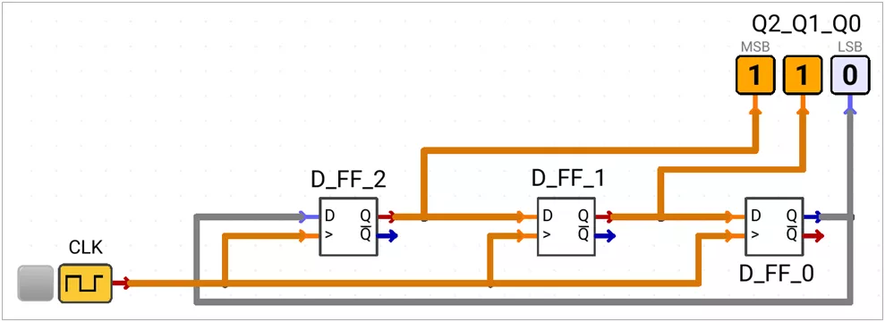
Clock | Q2_Q1_Q0 |
|---|---|
Initial | 110 |
↑ | 011 |
↑ | 101 |
↑ | 110 |
For this sequence, data moves Q2 → Q1 → Q0, and Q0 feeds back to D2.
Synchronous Data Loading:-
Each D input uses a 2:1 MUX. Parallel data loads only at the rising edge of Clock.
LD = 1: LoadP2_P1_P0.LD = 0: Shift the stored data.
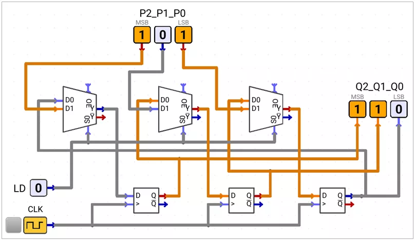
D2 = LD · P2 + LD' · Q0
D1 = LD · P1 + LD' · Q2
D0 = LD · P0 + LD' · Q1
Asynchronous Data Loading:-
PRESET and CLEAR load each bit without waiting for a clock edge.
LD = 1: LoadP2_P1_P0.LD = 0: Keep asynchronous controls inactive and shift normally.
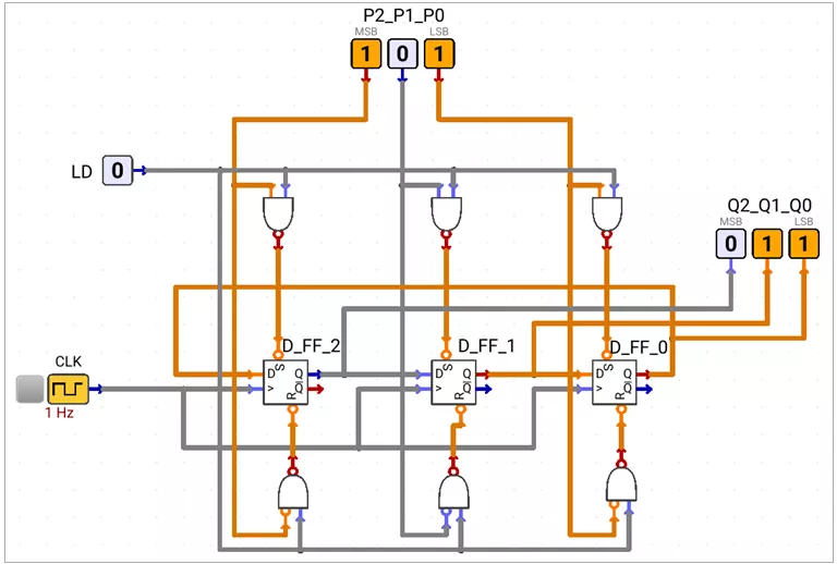
LD | Px | PREx' | CLRx' |
|---|---|---|---|
0 | X | 1 | 1 |
1 | 0 | 1 | 0 |
1 | 1 | 0 | 1 |
where x = 0, 1, 2.
PREx' = (LD · Px)' = LD' + bx'
CLRx' = (LD · Px')' = LD' + bx
Johnson's counter
A Johnson counter feeds the inverted last output back to the first input.
It is also called a twisted-ring counter or switch-tail ring counter.
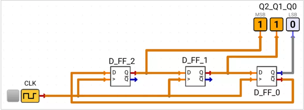
D2 = Q0'
D1 = Q2
D0 = Q1
Clock | Q2_Q1_Q0 |
|---|---|
Initial | 110 |
↑ | 111 |
↑ | 011 |
↑ | 001 |
↑ | 000 |
↑ | 100 |
↑ | 110 |
An n-bit Johnson counter has 2n valid states.
Controlled Ring/Johnson Counter
C selects normal or inverted feedback. LD selects loading or shifting.
C = 0: Ring mode;Q0feedsD2.C = 1: Johnson mode;Q0'feedsD2.LD = 1: LoadP2_P1_P0.LD = 0: Shift using the selected feedback.
D2 = LD · P2 + LD' · (Q0 ⊕ C)
D1 = LD · P1 + LD' · Q2
D0 = LD · P0 + LD' · Q1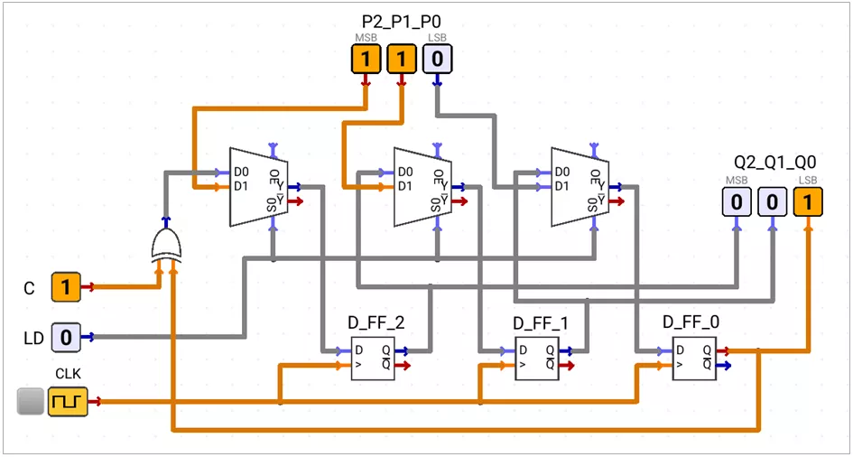
Applications of Registers and Counters
Registers and counters combine storage, event pulses, state counting, and control logic in practical digital systems.
Clock Gating Circuit
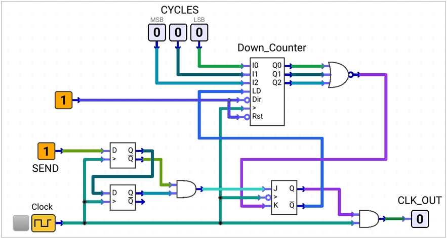
Main Blocks: Clock, edge detector, load/count-down counter, negative-edge JK flip-flop, zero detector, and AND clock gate.
Edge Detection:
SEND: 1 → 0 produces one active-HIGH pulse, SEND_EDGE. This pulse requests a new clock burst.
Counter control:
LD = ENABLE'.ENABLE = 0: LoadCYCLESinto the down counter.ENABLE = 1: Count down once per clock edge.- Note:
CYCLESmust be from001to111, corresponding to 1–7 output clock pulses.
Stop detection:
A NOR gate detects the zero state. STOP becomes HIGH when the counter reaches 000.
STOP = (Q2 + Q1 + Q0)'
CLK_OUT = Clock · ENABLE
Negative edge triggered JK Flip Flop:
J = SEND_EDGE, K = STOP, and Q = ENABLE. The flip-flop starts and stops the gated clock burst.
J = SEND_EDGE | K = STOP | ENABLE | Operation |
|---|---|---|---|
0 | 0 | 0 | Hold in idle |
1 | 0 | 1 | Set; burst starts |
0 | 0 | 1 | Hold until STOP appears |
0 | 1 | 0 | Reset; burst stops |
0 | 0 | 0 | Hold in idle |
Digital Dice
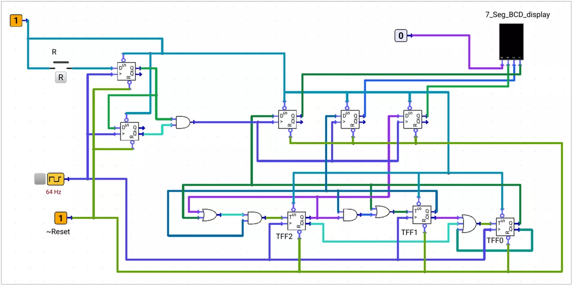
Main blocks: Edge detectors, MOD-6 counter, and PIPO register.
Edge Detectors:
A rising edge of the roll button produces one pulse. The pulse clocks the PIPO register only once.
MOD-6 Counter:
A fast counter continuously cycles through the six dice values.
001 → 010 → 011 → 100 → 101 → 110 → 001
T0 = Q0’ + Q1’ + Q2’
T1 = Q0 + Q2 · Q1
T2 = Q1 · (Q2 + Q0)
PIPO Register:
- Its parallel inputs receive the current MOD-6 counter value.
- The edge-detector pulse is its Clock input.
- Its output holds the captured value for the 7-segment display.
Target Landing Game:-
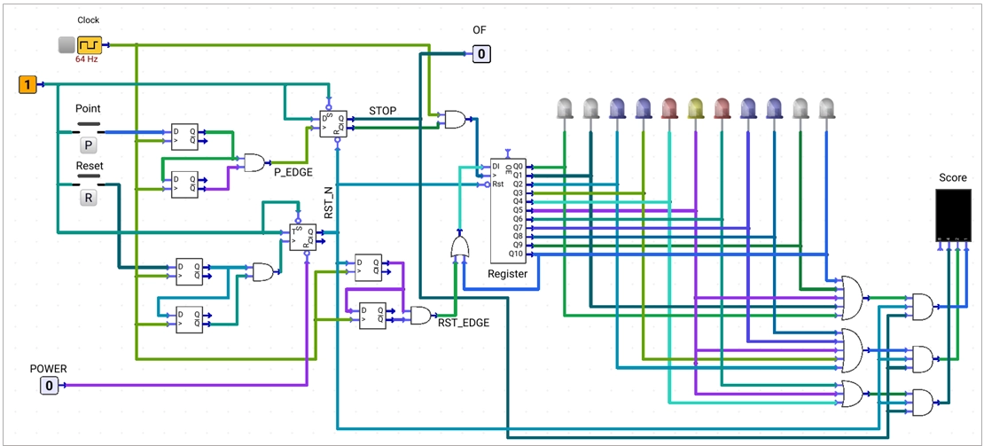
Main Building Blocks: Button edge detectors, run/reset control, clock gate, 11-bit ring counter, LED bank, and score logic.
Edge detector for P and R button and POWER:
P: 0 → 1generatesP_EDGE.R: 0 → 1generatesR_EDGE.POWERenables normal circuit operation.
Run/Reset toggling:
A T flip-flop uses T = 1, PRE' = 1, CLR' = POWER, and Q = RST_N.
POWER = CLR' | R_EDGE event | RST_N | Operation |
|---|---|---|---|
0 | X | 0 | Force reset mode |
1 | ↑ | Toggle | Change Run/Reset mode |
1 | No edge | Hold | Keep current mode |
Reset to Run edge:
RST_N: 0 → 1 generates one RST_EDGE pulse.
It inserts one HIGH bit into the ring counter.
STOP Logic:
A D flip-flop uses D = 1, PRE' = 1, CLR' = RST_N, and Clock = P_EDGE.
P_EDGE = 1storesSTOP = 1.STOPcloses the ring clock gate and makesOF = 1.- Further presses of
Pdo not move the selected position.
CLK_RING = Clock · RST_N · STOP'11-bit ring counter and led colours:
White → White → Blue → Blue → Red → Yellow → Red → Blue → Blue → White → WhiteD0 = Q10 + RST_EDGE: feedback continues the ring; the pulse inserts its first HIGH bit.RST_N = 0: all stages clear and the HIGH bit is removed.RST_N = 1: one HIGH bit circulates untilSTOP = 1.
Score Logic:
The stopped LED colour selects the displayed score:
Yellow = 7, Red = 4, Blue = 2, and White = 1.
b2 = STOP · RST_N · (YELLOW + RED)
b1 = STOP · RST_N · (YELLOW + BLUE)
b0 = STOP · RST_N · (YELLOW + WHITE)
The display shows 0 until P stores STOP = 1.
Note: In practical synchronous hardware, clock-enable or glitch-free clock-gating techniques are preferred.
Custom PWM generator
This circuit combines a register and counter to generate a stable PWM waveform. Input changes take effect only after the current eight-clock cycle finishes.
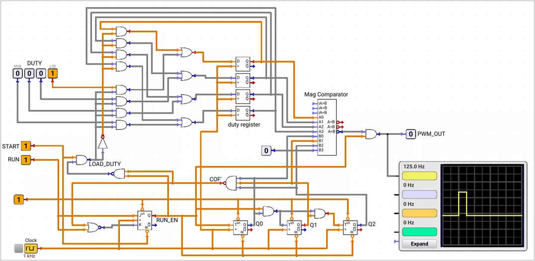
Main Blocks: START, RUN, Clock, DUTY, PWM_OUT, 4-bit duty register, 3-bit MOD-8 counter, 4-bit magnitude comparator, and PWM control circuit.
Input-output blocks and working:
START:- Active-HIGH circuit enable.
START = 0clears the controller and forces the PWM output LOW.
RUN:- Requests PWM operation.
- If it becomes LOW during a cycle, the circuit finishes that cycle before stopping.
Clock:- A 1 kHz clock drives the controller, register, and counter.
- Eight clock intervals form one 125 Hz PWM cycle.
DUTY:- A 4-bit value that requests the duty cycle.
- Values
0000to1000represent 0/8 to 8/8 HIGH intervals.
PWM_OUT:- Active-HIGH PWM output. It remains LOW while the controller is disabled or idle.
duty register:
The 4-bit register stores a stable duty value for the complete PWM cycle.
LOAD_DUTY selects loading or feedback holding.
LOAD_DUTY = 1: Capture the currentDUTYvalue on the rising clock edge.LOAD_DUTY = 0: Feed each register output back to its input and hold the value.
D_duty_reg[i] = LOAD_DUTY · DUTY[i] + LOAD_DUTY' · Q_duty_reg[i], i = 0…3MOD-8 Counter:
A 3-bit synchronous counter advances only while RUN_EN = 1. Its active-LOW clear input keeps the count at 000 during idle mode.
T0 = RUN_EN
T1 = RUN_EN · Q0
T2 = RUN_EN · Q0 · Q1
CLR' = RUN_EN
COF becomes HIGH at terminal count 111. The NAND output COF' provides its inverted form for the controller.
COF = Q2 · Q1 · Q0
COF' = (Q2 · Q1 · Q0)'
Control Logic:
A positive-edge-triggered JK flip-flop stores the operating state. Its output RUN_EN enables the counter and PWM output.
J = RUN
K = RUN' · COF = (RUN + COF')'
Q = RUN_EN
CLR' = START
LOAD_DUTY = START · (COF + RUN_EN')
LOAD_DUTY = START · (COF' · RUN_EN)'
RUN = 1 sets RUN_EN and starts PWM generation.
During a cycle, RUN_EN remains HIGH even if RUN becomes LOW.
RUN = 0 and COF = 1 reset the controller at the cycle boundary.
LOAD_DUTY is HIGH while idle or at COF = 1 so a new duty value never interrupts an active cycle.
4-bit Magnitude Comparator logic:
Comparator side A receives the duty-register value. Side B receives 0_Q2_Q1_Q0 from the counter.
The output (A < B) is active-LOW which becomes LOW when duty-register value is less than the count. Otherwise, it stays HIGH.
PWM_RAW = (A < B)'
PWM_OUT = PWM_RAW · RUN_EN
Duty Cycle of PWM:
Header Row represents the count value given to B [3:0] of the Mag Comparator.
Header Column represents the value in duty register given to A [3:0] of the Mag Comparator.
Each element shows PWM_RAW ((A<B)') after a clock edge.
| Duty Register (B) \ Count (A) | 0000 | 0001 | 0010 | 0011 | 0100 | 0101 | 0110 | 0111 | 1000 | 1001–1111 |
|---|---|---|---|---|---|---|---|---|---|---|
| 0000 | 0 | 1 | 1 | 1 | 1 | 1 | 1 | 1 | 1 | 1 |
| 0001 | 0 | 0 | 1 | 1 | 1 | 1 | 1 | 1 | 1 | 1 |
| 0010 | 0 | 0 | 0 | 1 | 1 | 1 | 1 | 1 | 1 | 1 |
| 0011 | 0 | 0 | 0 | 0 | 1 | 1 | 1 | 1 | 1 | 1 |
| 0100 | 0 | 0 | 0 | 0 | 0 | 1 | 1 | 1 | 1 | 1 |
| 0101 | 0 | 0 | 0 | 0 | 0 | 0 | 1 | 1 | 1 | 1 |
| 0110 | 0 | 0 | 0 | 0 | 0 | 0 | 0 | 1 | 1 | 1 |
| 0111 | 0 | 0 | 0 | 0 | 0 | 0 | 0 | 0 | 1 | 1 |
| PWM duty cycle (in %) | 0 | 12.5 | 25 | 37.5 | 50 | 62.5 | 75 | 87.5 | 100 | 100 |
The final output equals the table value only while RUN_EN = 1. Otherwise, PWM_OUT = 0.
Controlled Transmission Model
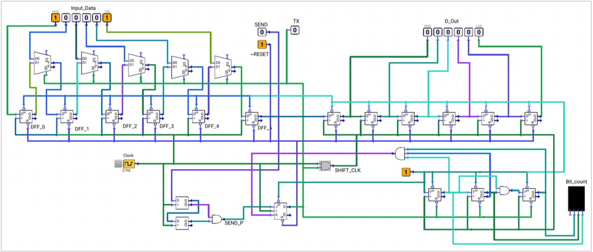
Main building blocks: PISO, SIPO, 3-bit counter, edge detector, and JK control flip-flop.
Inputs and outputs
SEND: 1 → 0requests a transmission.~Reset = 0resets the circuit and stored frame to000000.TX = 1shows that transmission is active.
PISO:
A 6-bit PISO uses a 2:1 MUX at each stage.
ENABLE = 0 loads the frame; ENABLE = 1 shifts one bit per common clock edge.
SIPO:
A 6-bit SIPO receives the serial data.
Its clock is SHIFT_CLK, and its parallel output is D_out.
SHIFT_CLK = Clock · ENABLEEdge detector:
An active-HIGH output falling-edge detector converts SEND: 1 → 0 into one HIGH SEND_P pulse.
JK Flip Flop:
The control flip-flop uses J = SEND_P, K = STOP, and Q = ENABLE.
SEND_P = 1setsENABLE = 1andTX = 1.- While
ENABLE = 1, furtherSENDchanges do not restart the frame. STOP = 1resetsENABLE, closes the clock gate, and returnsTXLOW.
3-bit counter:
CLR' = ENABLE: the counter is held at000while idle.ENABLE = 1:SHIFT_CLKadvances the counter.- The counter detects count
5so the sixth shift and control reset occur on the next active edge.
STOP = Q2 · Q1' · Q0