61. Latches and Flip Flops-ii
Question.1
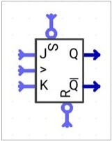
In the JK Flip-Flop circuit shown below, what is the purpose of the asynchronous S (PRESET) and R (CLEAR) inputs?
Select all correct options
In sequential circuits, the output depends on the present inputs and the previously stored state.
1-bit memory cell
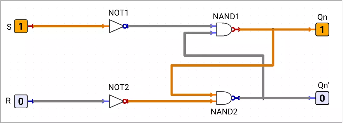
- NOT1 inverts S and NOT2 inverts R.
- Their outputs drive two cross-coupled NAND gates, whose feedback keeps the last output state after the input returns LOW.
- S = 1 sets Qn = 1, R = 1 resets Qn = 0, and S = R = 0 stores the previous state.
SR Latch: -
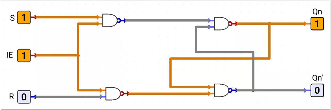
An active-HIGH input IE (Input Enable) controls when the SR latch can respond.
When IE = 0, the SR latch holds its previous state regardless of S and R.
| IE | S | R | Qₙ₊₁ | Qₙ₊₁’ | Operation |
|---|---|---|---|---|---|
| 0 | X | X | Qₙ | Q̅ₙ | Hold |
| 1 | 0 | 0 | Qₙ | Q̅ₙ | Hold |
| 1 | 1 | 0 | 1 | 0 | Set |
| 1 | 0 | 1 | 0 | 1 | Reset |
| 1 | 1 | 1 | 1 | 1 | Invalid |
X means don’t care
Invalid condition: When IE = 1 and S = R = 1, both outputs become HIGH, so Q and Q’ are no longer complementary. This is an invalid condition.
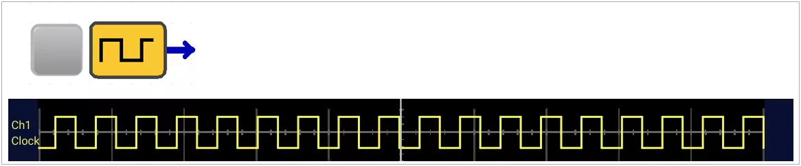
Clock Signal
A clock signal typically alternates periodically between logic 0 and logic 1.
It is commonly applied to a latch Enable input or to the clock input of a flip-flop.
JK Latch: -
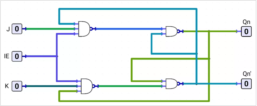
The JK latch removes the SR invalid input by using output feedback.
When J = K = 1, the feedback makes the stored state toggle instead of producing an invalid output.
| IE | J | K | Qₙ₊₁ | Operation |
|---|---|---|---|---|
| 0 | X | X | Qₙ | Hold |
| 1 | 0 | 0 | Qₙ | Hold |
| 1 | 0 | 1 | 0 | Reset |
| 1 | 1 | 0 | 1 | Set |
| 1 | 1 | 1 | Qₙ’ | Toggle / race-around risk |
Race-around condition:
In a level-triggered JK latch, J = K = 1 causes repeated toggling while the Enable/clock level remains active.
If the active clock-pulse width is greater than the propagation delay, Q can switch several times and its final state becomes uncertain.
Latches vs Flip Flops:-
- A latch is level-triggered: it can respond throughout the active Enable level.
- A flip-flop is edge-triggered: it updates only at the active clock edge.
| Feature | Latch | Flip-Flop |
|---|---|---|
| Activation | Signal level | Signal edge |
| Symbol identification | EN or IE input | > clock symbol |
| Output changes | During the active level | At the active edge |
| Input control | ENABLE | Clock |
| Main use | Level-sensitive storage | Edge-triggered storage |
An edge-triggered JK flip-flop solves the race-around problem because J and K are sampled only once at the active clock edge, allowing at most one toggle per edge.
Latches and Flip Flops Activation
| Active-HIGH or Positive edge | Active-LOW or Negative edge | |
|---|---|---|
| Level-triggered latch | Active while IE = 1. 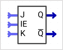 | Active while IE = 0. 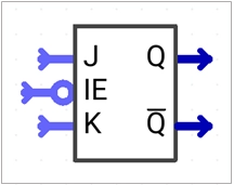 |
| Edge-triggered Flip Flop | Active at 0 → 1. 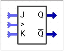 | Active at 1 → 0. 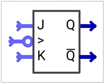 |
Latch applications
- Temporary data storage in level-sensitive data paths.
- Holding control or status signals while Enable is active.
Flip-flop applications
- Registers and counters.
- State storage in finite state machines (FSMs).
Excitation Tables
A truth table finds the output from known inputs.
An excitation table finds the inputs required for a desired output change.
SR Flip-Flop Excitation Table
| Qₙ | Qₙ₊₁ | S | R | Required action |
|---|---|---|---|---|
| 0 | 0 | 0 | X | Remain reset |
| 0 | 1 | 1 | 0 | Set |
| 1 | 0 | 0 | 1 | Reset |
| 1 | 1 | X | 0 | Remain set |
JK Flip-Flop Excitation Table
| Qₙ | Qₙ₊₁ | J | K | Required action |
|---|---|---|---|---|
| 0 | 0 | 0 | X | Remain reset |
| 0 | 1 | 1 | X | Set or toggle |
| 1 | 0 | X | 1 | Reset or toggle |
| 1 | 1 | X | 0 | Remain set |
D Flip Flop
A D flip-flop can be formed from a JK flip-flop by connecting D directly to J and D̅ to K.
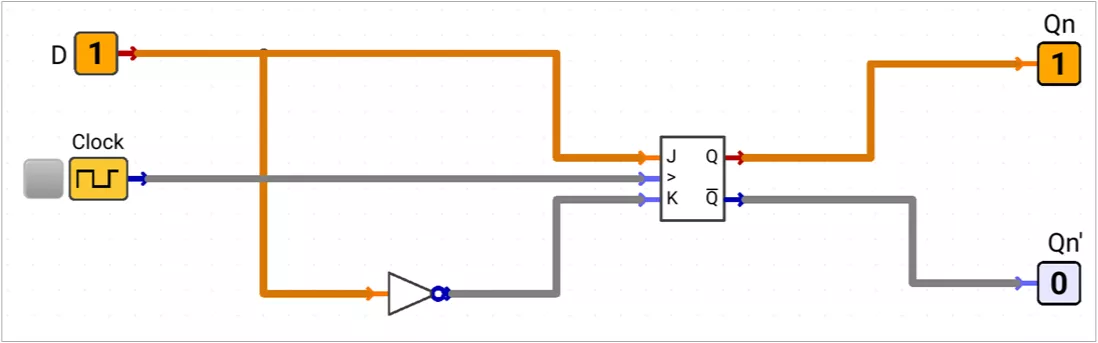
J = D
K = D̅
Qₙ₊₁ = D
Truth Table
| Clock | D | Qₙ₊₁ | Operation |
|---|---|---|---|
| Active edge | 0 | 0 | Store 0 |
| Active edge | 1 | 1 | Store 1 |
| No active edge | X | Qₙ | Hold |
Excitation Table
| Qₙ | Qₙ₊₁ | D |
|---|---|---|
| 0 | 0 | 0 |
| 0 | 1 | 1 |
| 1 | 0 | 0 |
| 1 | 1 | 1 |
D = Qₙ₊₁Applications
- Data registers and pipeline storage.
- One-bit data capture and building blocks for input synchronizer chains.
T Flip Flop
A T flip-flop can be formed from a JK flip-flop by connecting both J and K to T.
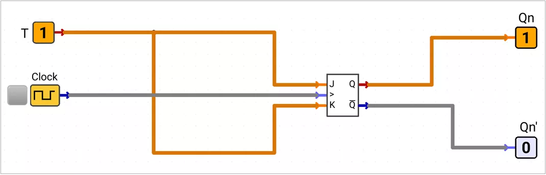
J = T
K = T
Qₙ₊₁ = T ⊕ Qₙ
Truth Table
| Clock | T | Qₙ₊₁ | Operation |
|---|---|---|---|
| Active edge | 0 | Qₙ | Hold |
| Active edge | 1 | Qₙ’ | Toggle |
| Non-active edge | X | Qₙ | Hold |
Excitation Table
| Qₙ | Qₙ₊₁ | T |
|---|---|---|
| 0 | 0 | 0 |
| 0 | 1 | 1 |
| 1 | 0 | 1 |
| 1 | 1 | 0 |
T = Qₙ ⊕ Qₙ₊₁Applications
- Binary counters.
- When T = 1, Q toggles on every active clock edge, producing a divide-by-2 output.
Asynchronous Inputs:-
The shown PRESET and CLEAR inputs are active-LOW. PRE̅ = 0 asynchronously sets Q = 1, while CLR̅ = 0 asynchronously resets Q = 0, regardless of the clock or synchronous inputs.
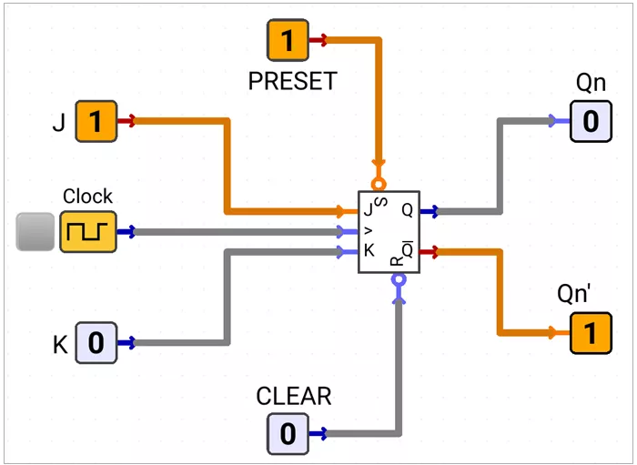
| P̅R̅E̅ | C̅L̅R̅ | Qₙ | Q̅ₙ | Operation |
|---|---|---|---|---|
| 1 | 1 | Qₙ | Q̅ₙ | Normal clocked operation |
| 0 | 1 | 1 | 0 | Asynchronous set |
| 1 | 0 | 0 | 1 | Asynchronous clear |
| 0 | 0 | 1 | 1 | Invalid / not allowed |
Flip Flop conversion:
- To convert one flip-flop into another
- list the target next-state behavior
- use the available flip-flop excitation table to find its required inputs
- simplify the input equations
- connect the circuit accordingly
Implementing T Flip Flop from D Flip Flop
For each T-flip-flop transition, D must equal the required next state Qₙ₊₁.
| T | Qₙ | Qₙ₊₁ | Required D |
|---|---|---|---|
| 0 | 0 | 0 | 0 |
| 0 | 1 | 1 | 1 |
| 1 | 0 | 1 | 1 |
| 1 | 1 | 0 | 0 |
D = T ⊕ Qₙ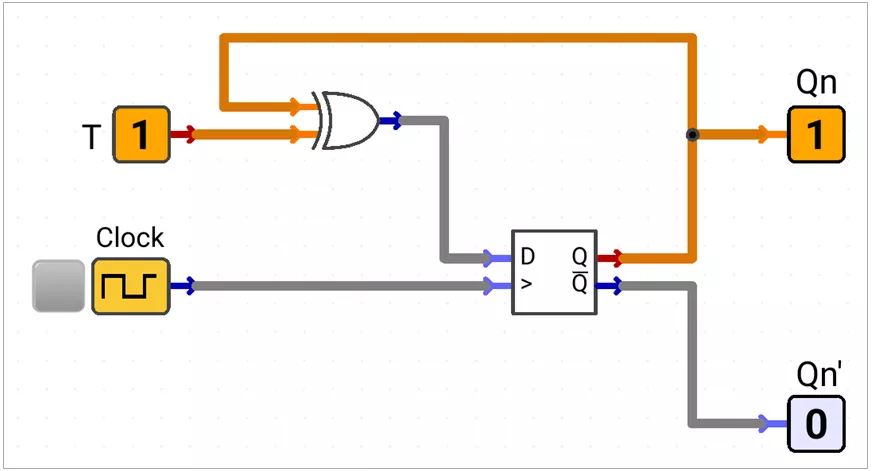
Flip-Flop Conversion Table
| Target Flip Flop | Available Flip Flop | Required connections |
|---|---|---|
| D | SR | S = D, R = D̅ |
| D | JK | J = D, K = D̅ |
| D | T | T = D ⊕ Qₙ |
| T | SR | S = T · Q̅ₙ, R = T · Qₙ |
| T | JK | J = T, K = T |
| T | D | D = T ⊕ Qₙ |
| JK | SR | S = J · Q̅ₙ, R = K · Qₙ |
| JK | T | T = J · Q̅ₙ + K · Qₙ |
| JK | D | D = J · Q̅ₙ + K̅ · Qₙ |
| SR | D | D = S + R̅ · Qₙ |
| SR | JK | J = S, K = R |
| SR | T | T = S · Q̅ₙ + R · Qₙ |
For conversions targeting an SR flip-flop, S = R = 1 remains prohibited.
Controlled D/T Flip Flop with inputs I and CNT
The JK input connections are J = I and K = I ⊕ CNT.
- When CNT = 0, the circuit behaves as a T flip-flop with T = I.
- When CNT = 1, it behaves as a D flip-flop with D = I.
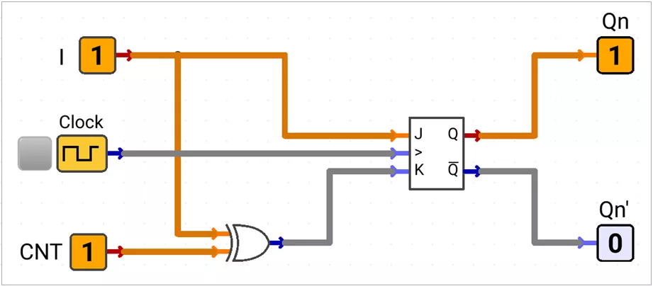
J = I
K = I ⊕ CNT
Truth Table
| CNT | I | Qₙ | Qₙ₊₁ | Operation |
|---|---|---|---|---|
| 0 | 0 | 0 | 0 | T mode: hold |
| 0 | 0 | 1 | 1 | T mode: hold |
| 0 | 1 | 0 | 1 | T mode: toggle |
| 0 | 1 | 1 | 0 | T mode: toggle |
| 1 | 0 | 0 | 0 | D mode: store 0 |
| 1 | 0 | 1 | 0 | D mode: store 0 |
| 1 | 1 | 0 | 1 | D mode: store 1 |
| 1 | 1 | 1 | 1 | D mode: store 1 |
Excitation Table
| CNT | Qₙ | Qₙ₊₁ | Required I | Behavior of I |
|---|---|---|---|---|
| 0 | 0 | 0 | 0 | T Behavior |
| 0 | 0 | 1 | 1 | T Behavior |
| 0 | 1 | 0 | 1 | T Behavior |
| 0 | 1 | 1 | 0 | T Behavior |
| 1 | 0 | 0 | 0 | D Behavior |
| 1 | 0 | 1 | 1 | D Behavior |
| 1 | 1 | 0 | 0 | D Behavior |
| 1 | 1 | 1 | 1 | D Behavior |
I = CNT · Qₙ₊₁ + C̅N̅T̅ · (Qₙ ⊕ Qₙ₊₁)JK Master Slave Flip Flop
A JK master-slave flip-flop uses two stages connected as Master → Slave.
- The master captures J and K during one clock level
- slave transfers the master state to
Qnduring the inverted clock level.
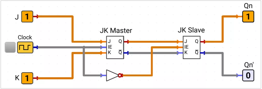
The Master and Slave operate on opposite clock levels, so only one stage is active at a time. This prevents the race-around condition.
- Clock = 1: Master active, Slave holds.
- Clock = 0: Master holds, Slave updates Qn.
QnandQn'are fed back to the Master input logic for JK operation.
Therefore, only one output change occurs per clock pulse, preventing race-around.
| J | K | Qₙ₊₁ | Operation |
|---|---|---|---|
0 | 0 | Qₙ | Hold |
0 | 1 | 0 | Reset |
1 | 0 | 1 | Set |
1 | 1 | Q̅ₙ | Toggle |