93. Target Landing Game Controller
Build a Target Landing Game Controller in which a single glowing LED moves rapidly across eleven colored LEDs. When the Point button is pressed, the movement must stop and the score of the selected LED must appear on the Score display.
Complete the control, reset, ring-feedback, stopping, and score-decoding circuits around the provided 11-bit shift register.
Given Components:
- POWER input for circuit initialization
- Clock operating at 64 Hz
- Reset push button operated using the R key
- Point push button operated using the P key
- One terminal of each push button connected to constant HIGH
- 11-bit shift register connected to LEDs in this pattern:
White, White, Blue, Blue, Red, Yellow, Red, Blue, Blue, White, White
- Score 7-segment BCD display
- OF 1-bit digital output
Constraints:
- Use rising-edge detection for the Reset and Point buttons so that each press produces one control pulse.
- When POWER = 0, initialize the complete circuit and clear all LEDs, Score, OF, and control states.
- Each valid Reset press must alternate the circuit between reset mode and normal mode.
- In reset mode, all shift-register bits must remain 0. Changing from reset mode to normal mode must insert exactly one HIGH bit into the register.
- During normal operation, the HIGH bit must circulate continuously through the LEDs using the 64 Hz Clock.
- The first valid Point press must stop the movement and keep the selected LED ON. Further presses must not change or restart the game.
- Keep OF = 0 before stopping and set OF = 1 after the first valid Point press.
- Keep Score = 0 while powered off, in reset mode, or while the LED is moving.
- After stopping, display the score based on the selected LED:
- White: 1
- Blue: 2
- Red: 4
- Yellow: 7
Expected Working Behaviour
After leaving reset mode, one HIGH bit circulates through the eleven LEDs. Pressing Point once freezes the selected LED, sets OF HIGH, and displays its score.
Registers store or shift binary data.
Counters move through a defined sequence of states.
Together, they support timing, control, transmission, and interactive circuits.
Ring Counter
A ring counter feeds the last flip-flop output back to the first flip-flop input.
The stored pattern circulates on each rising edge of Clock.
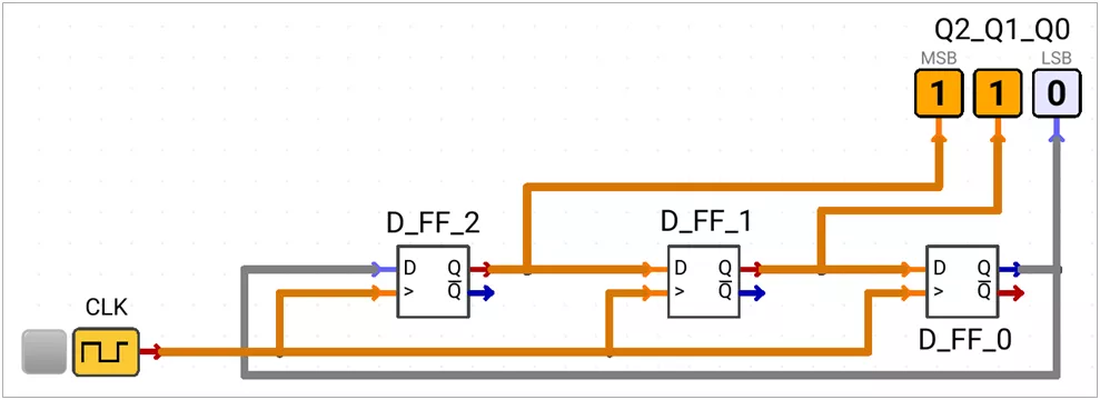
Clock | Q2_Q1_Q0 |
|---|---|
Initial | 110 |
↑ | 011 |
↑ | 101 |
↑ | 110 |
For this sequence, data moves Q2 → Q1 → Q0, and Q0 feeds back to D2.
Synchronous Data Loading:-
Each D input uses a 2:1 MUX. Parallel data loads only at the rising edge of Clock.
LD = 1: LoadP2_P1_P0.LD = 0: Shift the stored data.
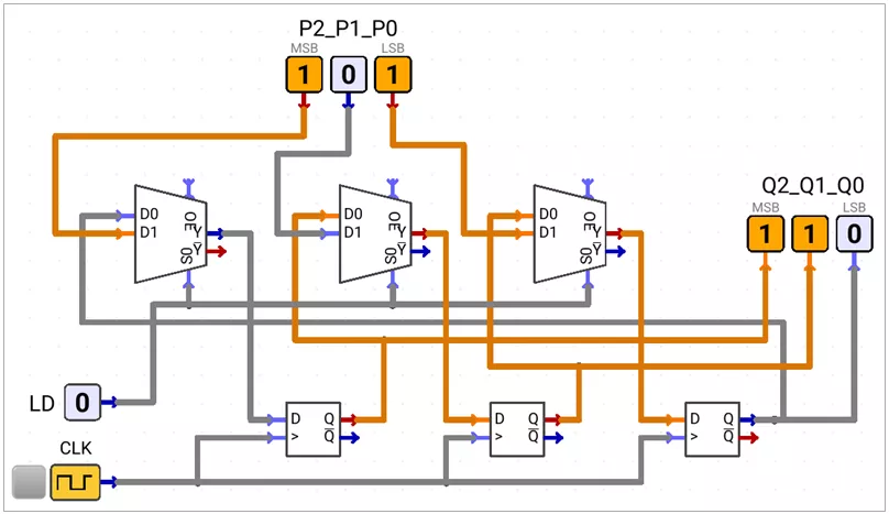
D2 = LD · P2 + LD' · Q0
D1 = LD · P1 + LD' · Q2
D0 = LD · P0 + LD' · Q1
Asynchronous Data Loading:-
PRESET and CLEAR load each bit without waiting for a clock edge.
LD = 1: LoadP2_P1_P0.LD = 0: Keep asynchronous controls inactive and shift normally.
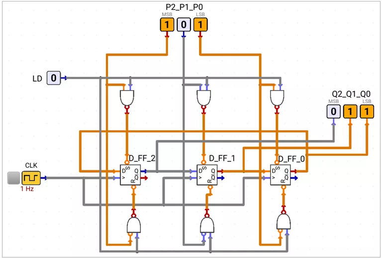
LD | Px | PREx' | CLRx' |
|---|---|---|---|
0 | X | 1 | 1 |
1 | 0 | 1 | 0 |
1 | 1 | 0 | 1 |
where x = 0, 1, 2.
PREx' = (LD · Px)' = LD' + bx'
CLRx' = (LD · Px')' = LD' + bx
Johnson's counter
A Johnson counter feeds the inverted last output back to the first input.
It is also called a twisted-ring counter or switch-tail ring counter.
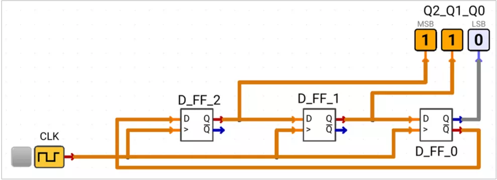
D2 = Q0'
D1 = Q2
D0 = Q1
Clock | Q2_Q1_Q0 |
|---|---|
Initial | 110 |
↑ | 111 |
↑ | 011 |
↑ | 001 |
↑ | 000 |
↑ | 100 |
↑ | 110 |
An n-bit Johnson counter has 2n valid states.
Controlled Ring/Johnson Counter
C selects normal or inverted feedback. LD selects loading or shifting.
C = 0: Ring mode;Q0feedsD2.C = 1: Johnson mode;Q0'feedsD2.LD = 1: LoadP2_P1_P0.LD = 0: Shift using the selected feedback.
D2 = LD · P2 + LD' · (Q0 ⊕ C)
D1 = LD · P1 + LD' · Q2
D0 = LD · P0 + LD' · Q1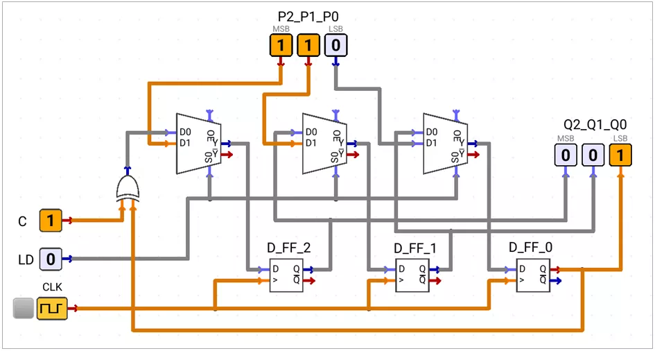
Applications of Registers and Counters
Registers and counters combine storage, event pulses, state counting, and control logic in practical digital systems.
Clock Gating Circuit
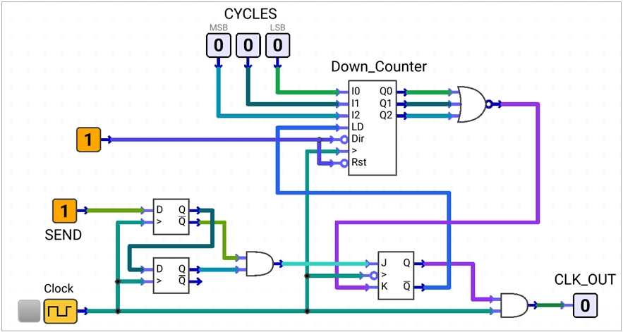
Main Blocks: Clock, edge detector, load/count-down counter, negative-edge JK flip-flop, zero detector, and AND clock gate.
Edge Detection:
SEND: 1 → 0 produces one active-HIGH pulse, SEND_EDGE. This pulse requests a new clock burst.
Counter control:
LD = ENABLE'.ENABLE = 0: LoadCYCLESinto the down counter.ENABLE = 1: Count down once per clock edge.- Note:
CYCLESmust be from001to111, corresponding to 1–7 output clock pulses.
Stop detection:
A NOR gate detects the zero state. STOP becomes HIGH when the counter reaches 000.
STOP = (Q2 + Q1 + Q0)'
CLK_OUT = Clock · ENABLE
Negative edge triggered JK Flip Flop:
J = SEND_EDGE, K = STOP, and Q = ENABLE. The flip-flop starts and stops the gated clock burst.
J = SEND_EDGE | K = STOP | ENABLE | Operation |
|---|---|---|---|
0 | 0 | 0 | Hold in idle |
1 | 0 | 1 | Set; burst starts |
0 | 0 | 1 | Hold until STOP appears |
0 | 1 | 0 | Reset; burst stops |
0 | 0 | 0 | Hold in idle |
Digital Dice
Main blocks: Edge detectors, MOD-6 counter, and PIPO register.
Edge Detectors:
A rising edge of the roll button produces one pulse. The pulse clocks the PIPO register only once.
MOD-6 Counter:
A fast counter continuously cycles through the six dice values.
001 → 010 → 011 → 100 → 101 → 110 → 001
T0 = Q0’ + Q1’ + Q2’
T1 = Q0 + Q2 · Q1
T2 = Q1 · (Q2 + Q0)
PIPO Register:
- Its parallel inputs receive the current MOD-6 counter value.
- The edge-detector pulse is its Clock input.
- Its output holds the captured value for the 7-segment display.
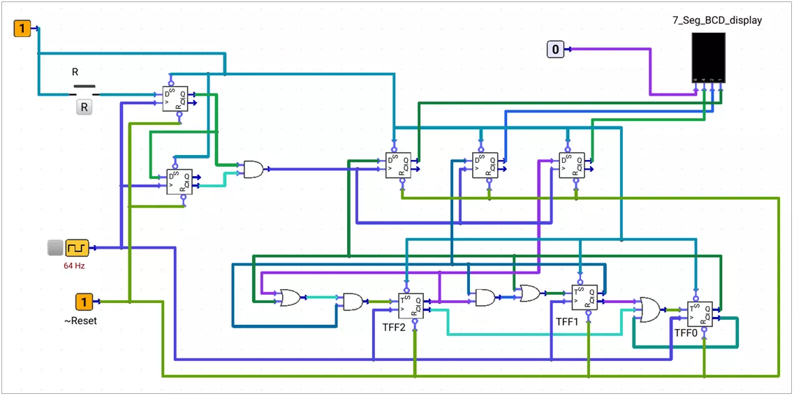
Target Landing Game:-
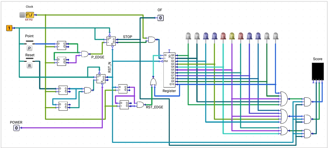
Main Building Blocks: Button edge detectors, run/reset control, clock gate, 11-bit ring counter, LED bank, and score logic.
Edge detector for P and R button and POWER:
P: 0 → 1generatesP_EDGE.R: 0 → 1generatesR_EDGE.POWERenables normal circuit operation.
Run/Reset toggling:
A T flip-flop uses T = 1, PRE' = 1, CLR' = POWER, and Q = RST_N.
POWER = CLR' | R_EDGE event | RST_N | Operation |
|---|---|---|---|
0 | X | 0 | Force reset mode |
1 | ↑ | Toggle | Change Run/Reset mode |
1 | No edge | Hold | Keep current mode |
Reset to Run edge:
RST_N: 0 → 1 generates one RST_EDGE pulse.
It inserts one HIGH bit into the ring counter.
STOP Logic:
A D flip-flop uses D = 1, PRE' = 1, CLR' = RST_N, and Clock = P_EDGE.
P_EDGE = 1storesSTOP = 1.STOPcloses the ring clock gate and makesOF = 1.- Further presses of
Pdo not move the selected position.
CLK_RING = Clock · RST_N · STOP'11-bit ring counter and led colours:
White → White → Blue → Blue → Red → Yellow → Red → Blue → Blue → White → WhiteD0 = Q10 + RST_EDGE: feedback continues the ring; the pulse inserts its first HIGH bit.RST_N = 0: all stages clear and the HIGH bit is removed.RST_N = 1: one HIGH bit circulates untilSTOP = 1.
Score Logic:
The stopped LED colour selects the displayed score:
Yellow = 7, Red = 4, Blue = 2, and White = 1.
b2 = STOP · RST_N · (YELLOW + RED)
b1 = STOP · RST_N · (YELLOW + BLUE)
b0 = STOP · RST_N · (YELLOW + WHITE)
The display shows 0 until P stores STOP = 1.
Note: In practical synchronous hardware, clock-enable or glitch-free clock-gating techniques are preferred.
Custom PWM generator
This circuit combines a register and counter to generate a stable PWM waveform. Input changes take effect only after the current eight-clock cycle finishes.
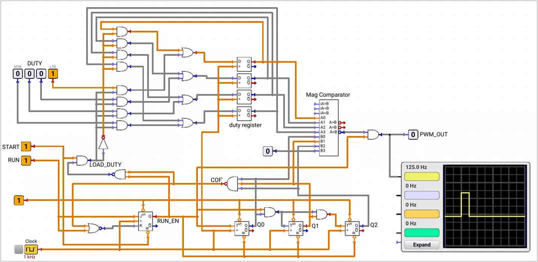
Main Blocks: START, RUN, Clock, DUTY, PWM_OUT, 4-bit duty register, 3-bit MOD-8 counter, 4-bit magnitude comparator, and PWM control circuit.
Input-output blocks and working:
START:- Active-HIGH circuit enable.
START = 0clears the controller and forces the PWM output LOW.
RUN:- Requests PWM operation.
- If it becomes LOW during a cycle, the circuit finishes that cycle before stopping.
Clock:- A 1 kHz clock drives the controller, register, and counter.
- Eight clock intervals form one 125 Hz PWM cycle.
DUTY:- A 4-bit value that requests the duty cycle.
- Values
0000to1000represent 0/8 to 8/8 HIGH intervals.
PWM_OUT:- Active-HIGH PWM output. It remains LOW while the controller is disabled or idle.
duty register:
The 4-bit register stores a stable duty value for the complete PWM cycle.
LOAD_DUTY selects loading or feedback holding.
LOAD_DUTY = 1: Capture the currentDUTYvalue on the rising clock edge.LOAD_DUTY = 0: Feed each register output back to its input and hold the value.
D_duty_reg[i] = LOAD_DUTY · DUTY[i] + LOAD_DUTY' · Q_duty_reg[i], i = 0…3MOD-8 Counter:
A 3-bit synchronous counter advances only while RUN_EN = 1. Its active-LOW clear input keeps the count at 000 during idle mode.
T0 = RUN_EN
T1 = RUN_EN · Q0
T2 = RUN_EN · Q0 · Q1
CLR' = RUN_EN
COF becomes HIGH at terminal count 111. The NAND output COF' provides its inverted form for the controller.
COF = Q2 · Q1 · Q0
COF' = (Q2 · Q1 · Q0)'
Control Logic:
A positive-edge-triggered JK flip-flop stores the operating state. Its output RUN_EN enables the counter and PWM output.
J = RUN
K = RUN' · COF = (RUN + COF')'
Q = RUN_EN
CLR' = START
LOAD_DUTY = START · (COF + RUN_EN')
LOAD_DUTY = START · (COF' · RUN_EN)'
RUN = 1 sets RUN_EN and starts PWM generation.
During a cycle, RUN_EN remains HIGH even if RUN becomes LOW.
RUN = 0 and COF = 1 reset the controller at the cycle boundary.
LOAD_DUTY is HIGH while idle or at COF = 1 so a new duty value never interrupts an active cycle.
4-bit Magnitude Comparator logic:
Comparator side A receives the duty-register value. Side B receives 0_Q2_Q1_Q0 from the counter.
The output (A < B) is active-LOW which becomes LOW when duty-register value is less than the count. Otherwise, it stays HIGH.
PWM_RAW = (A < B)'
PWM_OUT = PWM_RAW · RUN_EN
Duty Cycle of PWM:
Header Row represents the count value given to B [3:0] of the Mag Comparator.
Header Column represents the value in duty register given to A [3:0] of the Mag Comparator.
Each element shows PWM_RAW ((A<B)') after a clock edge.
| Duty Register (B) \ Count (A) | 0000 | 0001 | 0010 | 0011 | 0100 | 0101 | 0110 | 0111 | 1000 | 1001–1111 |
|---|---|---|---|---|---|---|---|---|---|---|
| 0000 | 0 | 1 | 1 | 1 | 1 | 1 | 1 | 1 | 1 | 1 |
| 0001 | 0 | 0 | 1 | 1 | 1 | 1 | 1 | 1 | 1 | 1 |
| 0010 | 0 | 0 | 0 | 1 | 1 | 1 | 1 | 1 | 1 | 1 |
| 0011 | 0 | 0 | 0 | 0 | 1 | 1 | 1 | 1 | 1 | 1 |
| 0100 | 0 | 0 | 0 | 0 | 0 | 1 | 1 | 1 | 1 | 1 |
| 0101 | 0 | 0 | 0 | 0 | 0 | 0 | 1 | 1 | 1 | 1 |
| 0110 | 0 | 0 | 0 | 0 | 0 | 0 | 0 | 1 | 1 | 1 |
| 0111 | 0 | 0 | 0 | 0 | 0 | 0 | 0 | 0 | 1 | 1 |
| PWM duty cycle (in %) | 0 | 12.5 | 25 | 37.5 | 50 | 62.5 | 75 | 87.5 | 100 | 100 |
The final output equals the table value only while RUN_EN = 1. Otherwise, PWM_OUT = 0.
Controlled Transmission Model
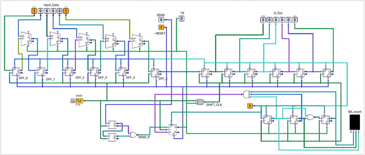
Main building blocks: PISO, SIPO, 3-bit counter, edge detector, and JK control flip-flop.
Inputs and outputs
SEND: 1 → 0requests a transmission.~Reset = 0resets the circuit and stored frame to000000.TX = 1shows that transmission is active.
PISO:
A 6-bit PISO uses a 2:1 MUX at each stage.
ENABLE = 0 loads the frame; ENABLE = 1 shifts one bit per common clock edge.
SIPO:
A 6-bit SIPO receives the serial data.
Its clock is SHIFT_CLK, and its parallel output is D_out.
SHIFT_CLK = Clock · ENABLEEdge detector:
An active-HIGH output falling-edge detector converts SEND: 1 → 0 into one HIGH SEND_P pulse.
JK Flip Flop:
The control flip-flop uses J = SEND_P, K = STOP, and Q = ENABLE.
SEND_P = 1setsENABLE = 1andTX = 1.- While
ENABLE = 1, furtherSENDchanges do not restart the frame. STOP = 1resetsENABLE, closes the clock gate, and returnsTXLOW.
3-bit counter:
CLR' = ENABLE: the counter is held at000while idle.ENABLE = 1:SHIFT_CLKadvances the counter.- The counter detects count
5so the sixth shift and control reset occur on the next active edge.
STOP = Q2 · Q1' · Q0