70. Digital Data Transmission
Question.7
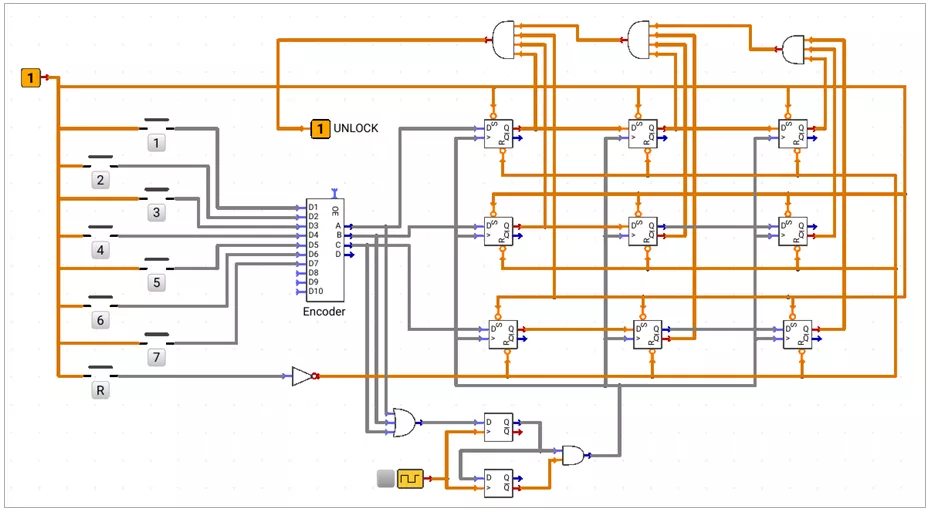
Your team has been assigned to develop a digital lock system using push buttons numbered 1 to 7 and a Reset (R) button.
Each key press is encoded into a 3-bit value and stored in a chain of registers. A pulse generation circuit updates the stored code whenever a new key is pressed, and a combinational logic block checks whether the entered sequence matches the unlock code.
The circuit developed by your team is shown below.
Select the design requirements that are correctly satisfied by this implementation.
A register is a group of flip-flops used to store a binary value. Each flip-flop stores one bit.
2-bit Register:-
A 2-bit register uses two D flip-flops to store one 2-bit value.
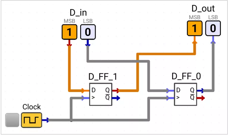
- D_FF_1 stores the most significant bit (MSB).
- D_FF_0 stores the least significant bit (LSB).
- Both bits are stored together at the rising edge of the clock.
Right Shift Register
A right shift register moves each stored bit from MSB to LSB at every active clock edge.
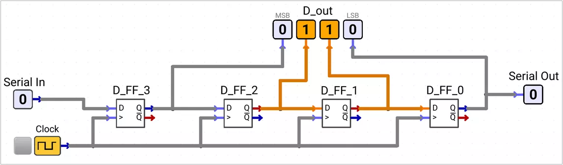
Serial In → Q3 → Q2 → Q1 → Q0 → Serial Out- Serial data enters at Q3 (MSB) from Serial In.
- Data leaves the register from Q0, the LSB.
Left Shift Register
A left shift register moves each stored bit from LSB to MSB at every active clock edge.
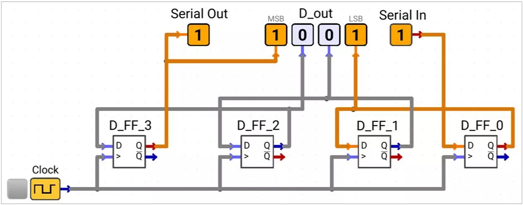
Serial In → Q0 → Q1 → Q2 → Q3 → Serial Out- Serial data enters at Q0 (LSB) from Serial In.
- Data leaves the register from Q3, the MSB.
Bi-directional Shift Register
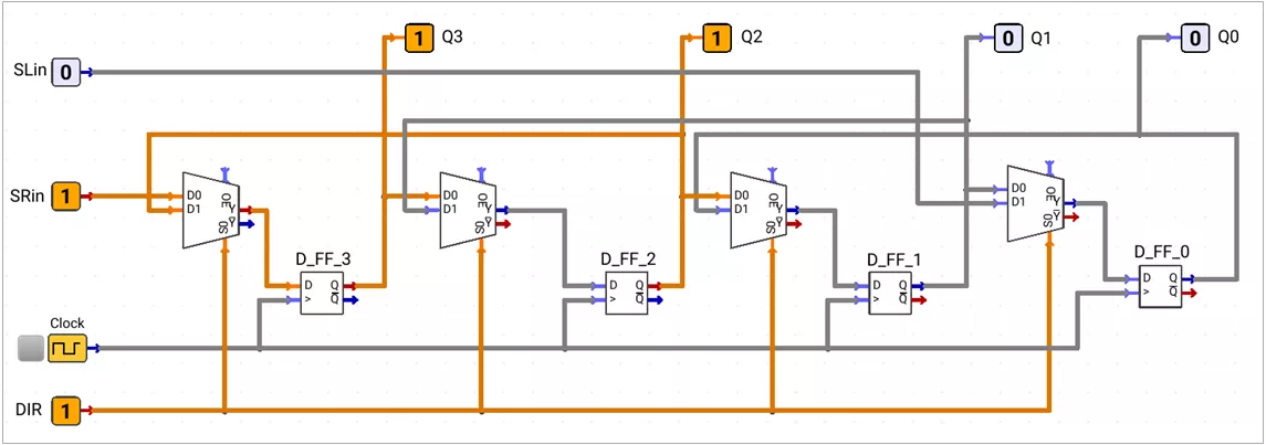
A bi-directional shift register moves data in either direction.
DIR = 0: selects right shift.DIR = 1: selects left shift.
DIR = 0: Right Shift | DIR = 1: Left Shift | Flip-Flop input |
|---|---|---|
SRin | Q2 | D3 |
Q3 | Q1 | D2 |
Q2 | Q0 | D1 |
Q1 | SLin | D0 |
SRinis the right-shift serial input.SLinis the left-shift serial input.
Edge Detector Circuit
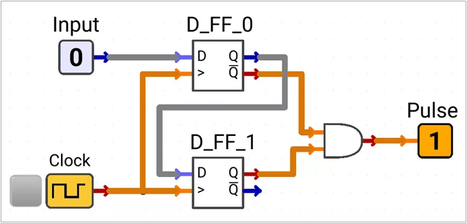
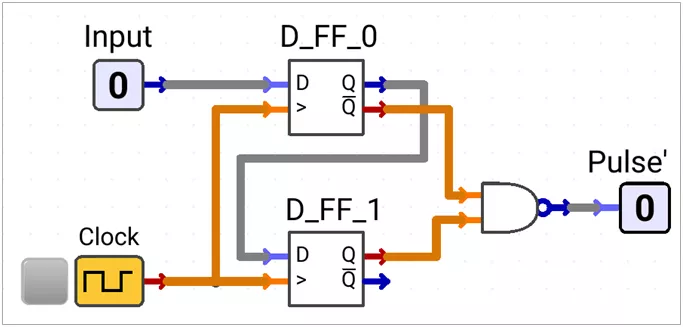
An edge detector is a sequential circuit that activates when the required input transition appears.
- Two D flip-flops store the current and previous input samples.
- Q0 is the current sampled input.
- Q1 is the previous sampled input.
- An AND gate gives an active-HIGH pulse.
- A NAND gate gives an active-LOW pulse.
Rising-edge active-HIGH = Q0 · Q₁’
Falling-edge active-HIGH = Q₀’· Q1| Rising Edge (0 → 1) | Falling Edge (1 → 0) | |
|---|---|---|
Active-HIGH output pulse Idle: 0 Active: 1 | 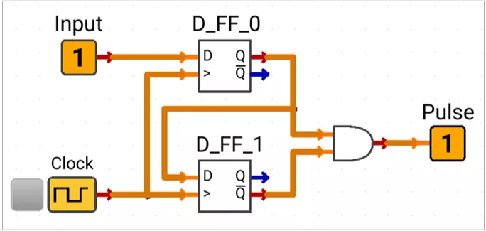
| 
|
Active-LOW output pulse Idle: 1 Active: 0 | 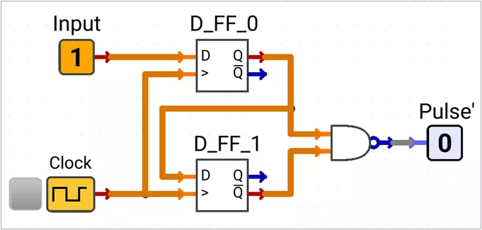
| 
|
Applications
- Push-button press detection.
- Single-clock pulse generation.
- Counter or register enable control.
- Event and interrupt detection.
Digital Data Transmission
Shift registers convert and transmit data in serial or parallel form.
| Type | Input method | Output method | Application |
|---|---|---|---|
PIPO | Parallel | Parallel | Data storage or bus buffer |
SISO | Serial | Serial | Digital delay line |
SIPO | Serial | Parallel | Serial data receiver |
PISO | Parallel | Serial | Serial data transmitter |
Parallel-In Parallel-Out (PIPO)
All input bits are loaded together and appear together at the outputs.
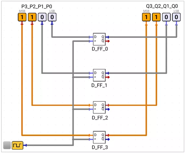
P3_P2_P1_P0 → Q3_Q2_Q1_Q0Serial-In Serial-Out (SISO)
Bits enter and leave one at a time. A 4-bit SISO delays the first bit by four active clock edges.
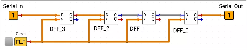
Serial In → Q3 → Q2 → Q1 → Q0 → Serial OutSerial-In Parallel-Out
Bits enter serially. After four active clock edges, the 4-bit word is available at Q3 to Q0.
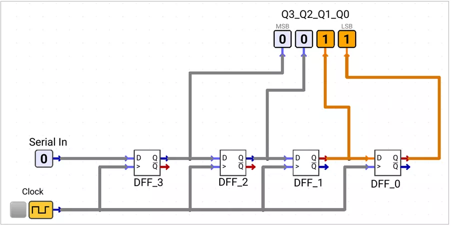
Serial In → Q3 → Q2 → Q1 → Q0Parallel-In Serial-Out
A PISO register loads a complete word and then shifts it out one bit at a time. It uses an additional LOAD input.
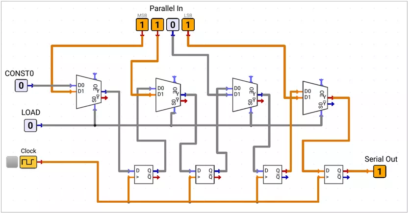
LOAD = 1: Parallel input data is loaded.LOAD = 0: Data is shifted towardSerial Out.
Parallel to Serial to Parallel Transmission
PISO → Transmission Line → SIPO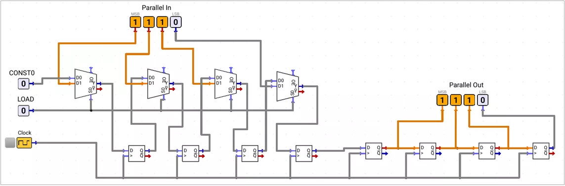
LOAD = 1: The PISO register loads the parallel data.LOAD = 0: The PISO register transmits one bit per active clock edge.- The SIPO register receives the bits and rebuilds the parallel word.
- A 4-bit word requires four active clock edges at the receiver.
Applications
- Communication between digital boards using fewer wires.
- Sensor or peripheral data transfer.
- Serial links between controllers and display drivers.
Register Applications:
LED Belt
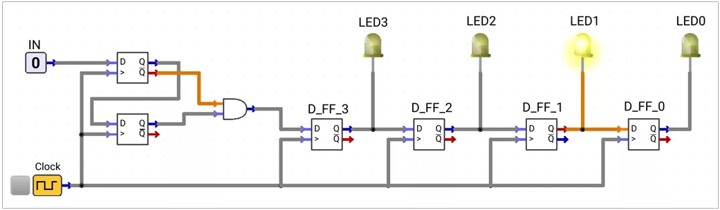
Circuit behaviour
- A sampled falling edge of
INgenerates a HIGH pulse, which is loaded intoQ3on the following active clock edge. - Each rising clock edge shifts it from Q3 to Q0, lighting one active-HIGH LED.
Functional table
| Clock event | IN | Q3 | Q2 | Q1 | Q0 | LED Glowing |
|---|---|---|---|---|---|---|
↑ | 1 | 0 | 0 | 0 | 0 | NONE |
↑ | 0 | 0 | 0 | 0 | 0 | NONE |
↑ | 0 | 1 | 0 | 0 | 0 | LED3 |
↑ | 0 | 0 | 1 | 0 | 0 | LED2 |
↑ | 0 | 0 | 0 | 1 | 0 | LED1 |
↑ | 0 | 0 | 0 | 0 | 1 | LED0 |
↑ = rising clock edge.
Digital Lock
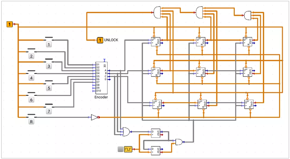
Implementation:
- Input selection:
- Buttons 1 to 7 drive D1 to D7 of a 10:4 encoder.
- Outputs A, B, and C form the 3-bit code; D is unused.
- Button press detection:
- When no button is pressed, the encoder outputs
0000. - Since only buttons 1–7 are used, every valid button code makes at least one of A, B, or C HIGH.
- Therefore,
(A + B + C)detects a button press using only a 3-input OR gate. - A rising-edge detector converts this signal into one short storage pulse.
- When no button is pressed, the encoder outputs
- Sequence storage:
- Three 3-bit PIPO stages store the last three button codes.
- Each new code advances the older codes by one stage.
- Code matching: Combinational AND logic checks the stored sequence
5, 1, 7.It setsUNLOCK = 1only for this sequence. - Reset:
Ris inverted before reaching the active-LOW CLR inputs. PressingRclears every PIPO stage.
Working
- Press 5, then 1, then 7.
- Each press creates one pulse and stores the encoded 3-bit value.
- After the third correct value, the matching logic sets
UNLOCK = 1. - A wrong sequence keeps
UNLOCK = 0. PressRto clear the stored sequence.
5 → 1 → 7 → UNLOCK = 1