Digital Register Quick Reference Guide

Basic Concept of Register
A register is a group of flip-flops used to store a binary value.
- Each flip-flop stores 1 bit.
- All flip-flops normally use a common clock.
- An n-bit register requires n flip-flops.
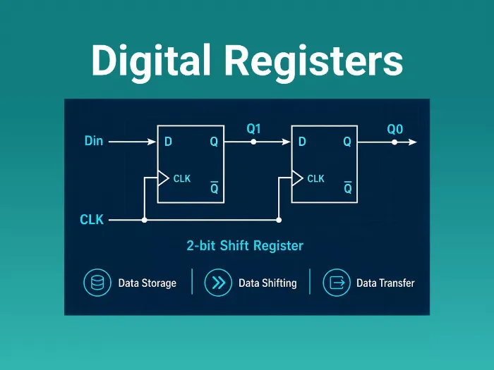
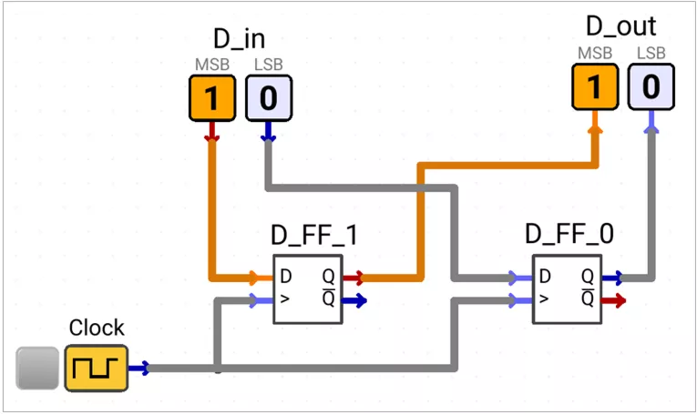
2-Bit Register Example
A 2-bit register contains two D flip-flops:
D1stores the MSB.D0stores the LSB.- Outputs are
Q1andQ0.
Both flip-flops receive the same clock signal.
Fig. 1: 2-bit Register

Working
- Before the active clock edge, the register keeps its previous value.
- At the active clock edge,
D1D0is stored inQ1Q0. - The stored value remains unchanged until the next active clock edge.
Table 1: 2-Bit Register Example
| Condition | D1D0 | Q1Q0 |
|---|---|---|
| Before clock edge | 10 | Previous value |
| At active clock edge | 10 | 10 |
| After clock edge | X | 10 |
X means the input value does not affect the already stored output.
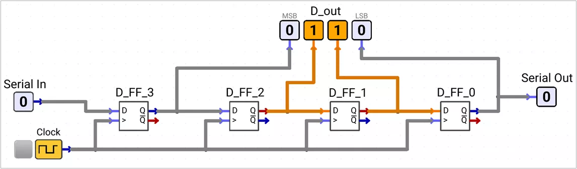
Right Shift Register
A right shift register moves every stored bit one position toward the LSB.
For a 4-bit register:
Q3 → Q2 → Q1 → Q0Here:
Q3is theMSB.Q0is theLSB.- New serial data enters
Q3. - Data leaves from
Q0.
Fig. 2: 4-bit Right Shift Register

Connections
D3=Serial InD2=Q3D1=Q2D0=Q1Serial Out=Q0
Working
At every active clock edge:
Q3receives the serial input.Q2receives the previousQ3.Q1receives the previousQ2.Q0receives the previousQ1.
Table 2: Right Shift Example
| Present Value | Serial Input | Value After Clock |
|---|---|---|
| 1011 | 0 | 0101 |
The bits move from MSB to LSB.
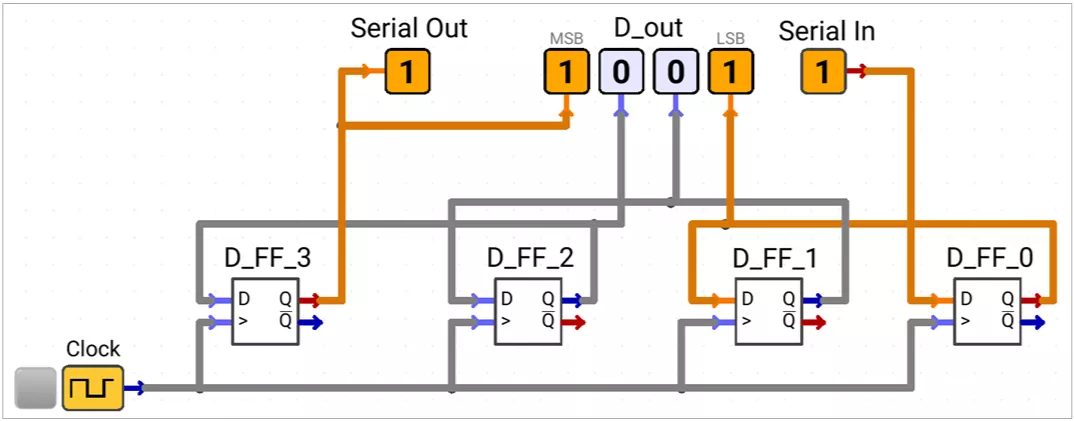
Left Shift Register
A left shift register moves every stored bit one position toward the MSB.
For a 4-bit register:
Q0 → Q1 → Q2 → Q3Here:
- New serial data enters
Q0. - Data leaves from
Q3.
Fig. 3: 4-bit Left Shift Register

Connections
D0=Serial InD1=Q0D2=Q1D3=Q2Serial Out=Q3
Working
At every active clock edge:
Q0receives the serial input.Q1receives the previousQ0.Q2receives the previousQ1.Q3receives the previousQ2.
Table 3: Left Shift Example
| Present Value | Serial Input | Value After Clock |
|---|---|---|
| 1011 | 0 | 0110 |
The bits move from LSB to MSB.
Edge Detector Circuit
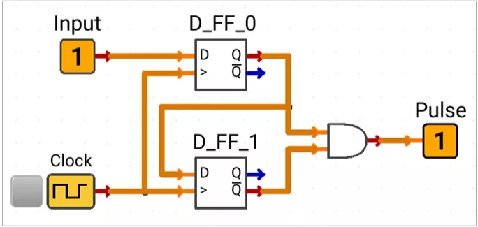
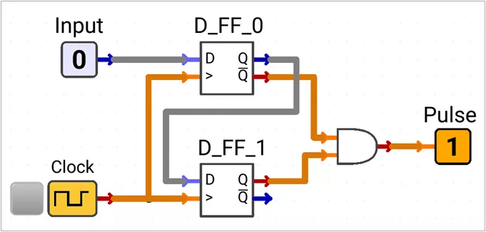
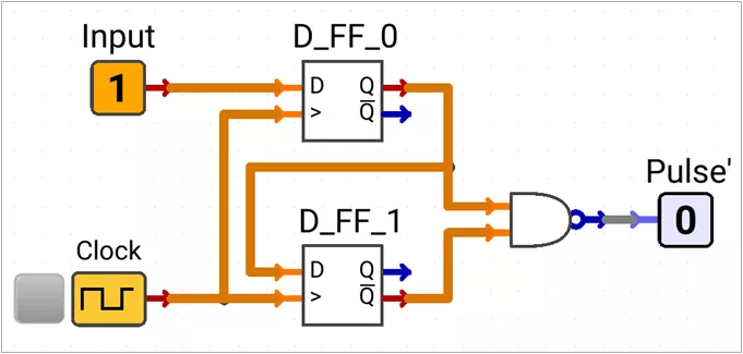
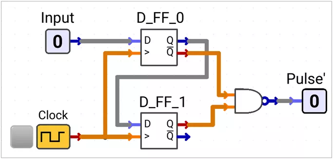
An edge detector produces a short pulse when an input signal changes from one logic level to another.
It uses two clocked samples:
Q0– current sampled inputQ1– previous sampled input
The output pulse normally remains active for one clock cycle.
Table 4: Edge Detector Types
| Rising Edge 0 → 1 | Falling Edge 1 → 0 | |
| Active-HIGH output | ![]() The output becomes 1 for one clock cycle when the input changes from 0 to 1. | ![]() The output becomes 1 for one clock cycle when the input changes from 1 to 0. |
| Active-LOW output | ![]() The output becomes 0 for one clock cycle when the input changes from 0 to 1. | ![]() The output becomes 0 for one clock cycle when the input changes from 1 to 0. |
Applications
- Detecting push-button presses
- Generating counter pulses
- Capturing data in registers
- Starting serial data transmission
- Detecting changes in control signals
- Generating one-clock enable pulses
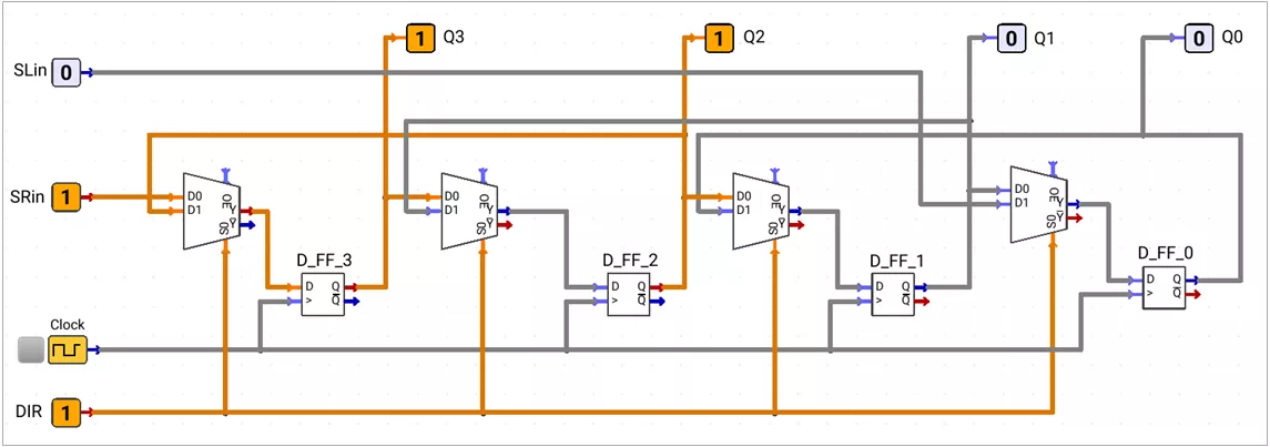
Bi-Directional Shift Register
A bi-directional shift register can shift data in both directions.
- Right shift:
MSBtoLSB - Left shift:
LSBtoMSB
A direction input DIR selects the shifting direction.
Fig. 4: 4-bit Bi-directional Shift Register with Two inputs

Circuit Structure
Each flip-flop input is connected to a 2-to-1 multiplexer.
The multiplexer selects:
- Data from the left-side flip-flop for right shifting
- Data from the right-side flip-flop for left shifting
Two serial inputs are used:
SRin– enters theMSBduring right shiftSLin– enters theLSBduring left shift
Table 5: Bi-Directional Register Connections
| Flip-Flop Input | DIR = 0 Right Shift | DIR = 1 Left Shift |
|---|---|---|
D3 | SRin | Q2 |
D2 | Q3 | Q1 |
D1 | Q2 | Q0 |
D0 | Q1 | SLin |
Working
When DIR = 0
- The multiplexers select the right-shift connections.
- Data moves from
Q3towardQ0. - New data enters through
SRin.
When DIR = 1
- The multiplexers select the left-shift connections.
- Data moves from
Q0towardQ3. - New data enters through
SLin.
The selected shift occurs at every active clock edge.
Register Input and Output Types
Registers are classified by how data enters and leaves them.
Table 6: Register Type Comparison
| Type | Input Method | Output Method | Main Function |
|---|---|---|---|
| PIPO | Parallel | Parallel | Store a complete binary word |
| SISO | Serial | Serial | Shift or delay serial data |
| SIPO | Serial | Parallel | Convert serial data to parallel |
| PISO | Parallel | Serial | Convert parallel data to serial |
PIPO Register
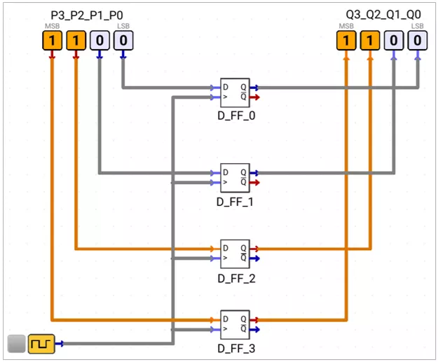
PIPO means Parallel-In Parallel-Out.
All input bits are loaded together, and all output bits are available together.
Fig. 5: Parallel-in Parallel-out Shift Register

Connections
- Each parallel input is connected to one D flip-flop.
- All flip-flops share a common clock.
- Each flip-flop provides a separate output.
Working
At the active clock edge:
Q3Q2Q1Q0 = P3P2P1P0The complete binary word is stored in one clock operation.
Functionality
- Temporary data storage
- Data buffering
- Processor registers
- Parallel data transfer
SISO Register
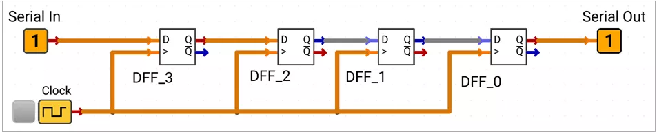
SISO means Serial-In Serial-Out.
Data enters one bit at a time and leaves one bit at a time.
Fig. 6: Serial-in Serial-out Shift Register

Connections
- The output of each flip-flop connects to the input of the next flip-flop.
- The first flip-flop receives the serial input.
- The last flip-flop provides the serial output.
Working
At each active clock edge:
- One new bit enters the register.
- Every stored bit moves one position.
- One bit leaves through the serial output.
For an n-bit SISO register, a bit reaches the output after n clock edges.
Functionality
- Serial data delay
- Digital delay lines
- Bit-by-bit data transfer
SIPO Register
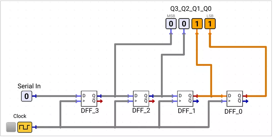
SIPO means Serial-In Parallel-Out.
Data enters one bit at a time, but all stored bits can be read together.
Fig. 7: Serial-in Parallel-out Shift Register

Connections
- The flip-flops are connected as a serial shift register.
- Each flip-flop output is also available as a parallel output.
Working
- One serial bit enters during each clock edge.
- The bits move through the register.
- After the required number of clock edges, the complete word is available at the parallel outputs.
Functionality
- Serial-to-parallel conversion
- LED control
- Expanding processor output pins
- Receiving serial data
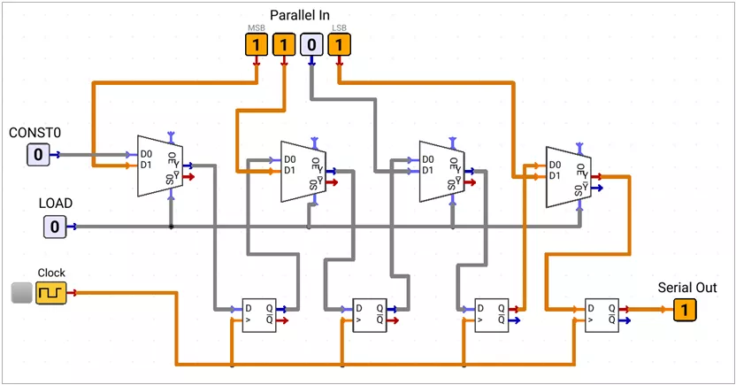
PISO Register
PISO means Parallel-In Serial-Out.
A complete binary word is loaded together and then shifted out one bit at a time.
Fig. 8: Parallel-in Serial-out Shift Register

Connections
Each flip-flop uses a multiplexer to select:
- Parallel input during load
- Previous flip-flop output during shift
A LOAD input controls the operation.
Working
When LOAD = 1
All parallel input bits are loaded together:
Q3Q2Q1Q0 = P3P2P1P0When LOAD = 0
The stored data shifts one bit during each clock edge.
For right shifting:
- Data moves toward
Q0. - Serial data leaves from
Q0.
Functionality
- Parallel-to-serial conversion
- Sending processor data over one wire
- Serial communication
- Reducing transmission wires
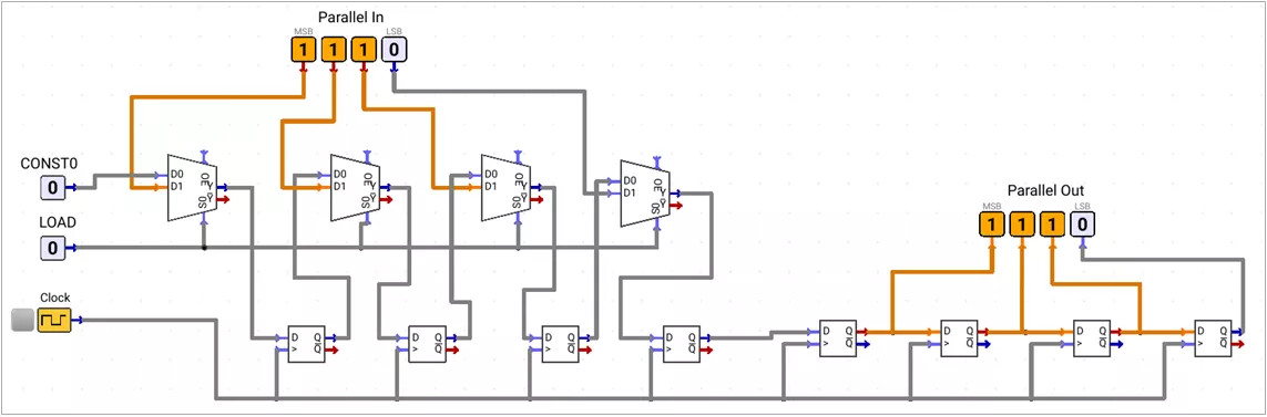
Parallel-to-Serial-to-Parallel Transmission
Parallel data can be transmitted through one serial line using:
PISO → Transmission Line → SIPO
Fig. 9: Parallel to Serial to Parallel Transmission

Working
- A parallel data word is loaded into the PISO register.
- The PISO register shifts out one bit during each clock cycle.
- The transmission line carries the bits one at a time.
- The SIPO register receives one bit during each clock cycle.
- After all bits are received, the original word appears at the parallel outputs.
Table 7: Data Transmission Stages
| Stage | Register or Link | Data Form |
|---|---|---|
| Input | PISO parallel inputs | Parallel |
| Conversion | PISO shifting | Parallel to serial |
| Transfer | Transmission line | Serial |
| Conversion | SIPO shifting | Serial to parallel |
| Output | SIPO parallel outputs | Parallel |
Important Conditions
- The transmitter and receiver must use the same bit order.
- The receiver must sample each bit at the correct clock time.
- The number of transmitted bits must match the register size.
Benefits
- Requires fewer transmission wires
- Suitable for longer-distance communication
- Reduces circuit connections
- Allows parallel devices to communicate through a serial link
Register Applications
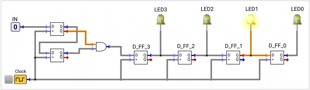
LED Belt
The LED belt uses a 4-bit right shift register to create a moving-light effect.
Each register output is connected to one active-HIGH LED:
Q3→ LED3Q2→ LED2Q1→ LED1Q0→ LED0
An active-HIGH output falling-edge detector monitors input IN.
Fig. 10: LED Belt Circuit

Circuit Behaviour
- Normally, the edge-detector output remains
0. - When IN changes from 1 → 0, the detector generates one HIGH pulse.
- This HIGH bit enters the serial input of the shift register.
- At every clock edge, the HIGH bit moves one position toward the
LSB. - The connected LEDs show the position of the stored HIGH bit.
Table 8: LED Belt Example
| Clock Event | Register Output Q3Q2Q1Q0 | Glowing LED |
|---|---|---|
| Falling edge detected | 1000 | LED3 |
| Next clock | 0100 | LED2 |
| Next clock | 0010 | LED1 |
| Next clock | 0001 | LED0 |
Only one HIGH pulse is inserted for one falling edge. Therefore, one LED moves through the belt after each clock.
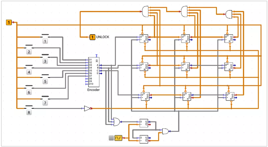
Digital Lock
The digital lock stores a sequence of three button presses and compares it with the correct code:
5 → 1 → 7
Input Section
The circuit contains seven push buttons labelled 1 to 7.
- A pressed button generates HIGH.
- Buttons are connected to encoder inputs
D1toD7. - The encoder produces outputs
A,B,C, andD. - Output
Dis unused. - Outputs
A,B, andCform the 3-bit button code.
Button-Press Detection
The signal: A + B + C
becomes HIGH when an encoded button value is present.
This signal is connected to an active-HIGH output rising-edge detector.
When a button is pressed:
- A + B + C changes from 0 → 1.
- The edge detector generates one HIGH pulse.
- This pulse is connected to the clock inputs of all PIPO registers.
- Only one register update occurs for each button press.
Sequence Storage
The circuit uses three 3-bit PIPO registers to store three encoded button values.
The registers store the entered button sequence. The stored values are checked after each entry.
Code Matching
A combinational circuit is connected after each PIPO register.
Each circuit produces HIGH only when its stored 3-bit value matches the required button value:
- First required value:
5 - Second required value:
1 - Third required value:
7
The three match signals are combined to generate UNLOCK.
Table 9: Digital Lock Code Check
| Stored Entry | Required Button | Match Output |
| First entry | 5 | HIGH when value is 5 |
| Second entry | 1 | HIGH when value is 1 |
| Third entry | 7 | HIGH when value is 7 |
When all three stored values match:
UNLOCK = 1
Reset Operation
The R push button shifts the code in next register. It works similar to "0".
Complete Working
- The user presses one button from 1 to 7.
- The encoder converts the button number into a 3-bit code.
- The rising-edge detector generates one clock pulse.
- The PIPO registers record the button entry.
- The process repeats for three button presses.
- The combinational circuits check the stored sequence.
UNLOCKbecomes HIGH only when the entered code is517.
Fig. 11: Digital Lock Circuit using Registers

Concept understood? Let's apply and learn for real