
22. Transistor Level Logic Gates
Question.4
Determine the Boolean expression implemented at output Y.
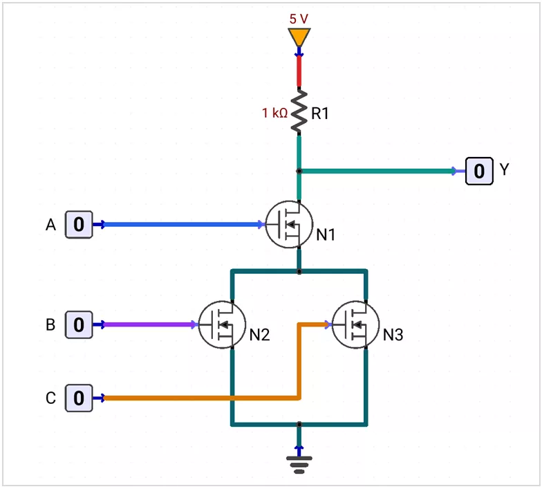
Logic gates are physically implemented using transistor switches. A transistor network creates a path either toward the supply or toward ground, producing logic 1 or logic 0.
Note: The circuits shown are simplified for learning; practical IC implementations may use optimized transistor networks.
How Transistors Create Logic
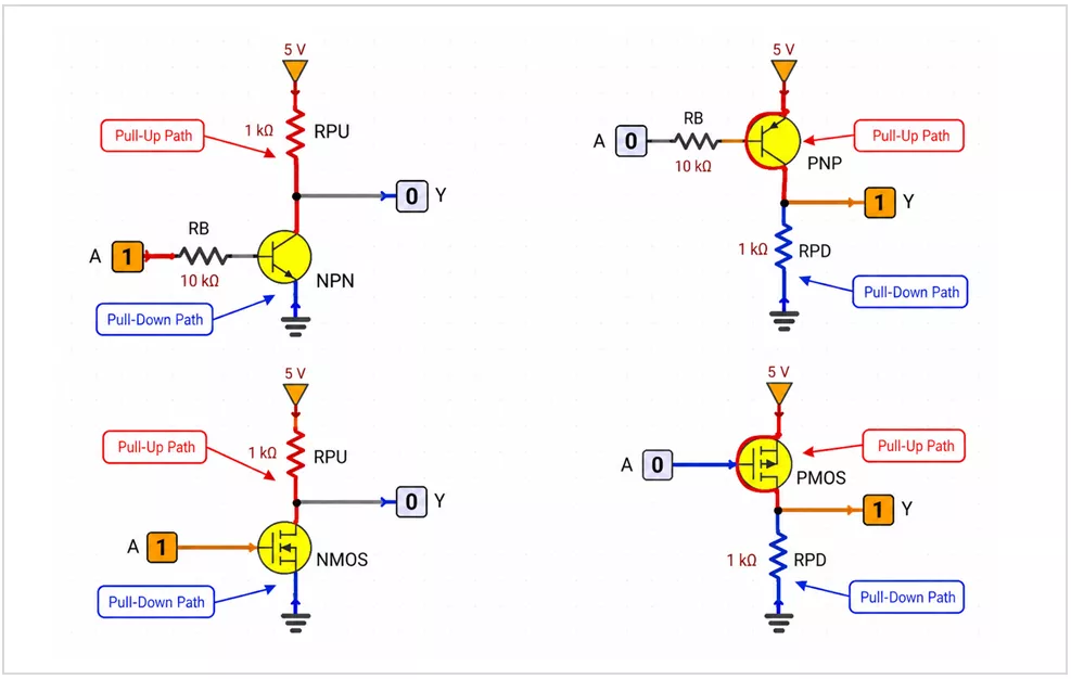
Pull-Up and Pull-Down Paths
- Pull-up connects Y toward VCC/VDD → 1.
- Pull-down connects Y toward ground → 0.
Series and Parallel Connections
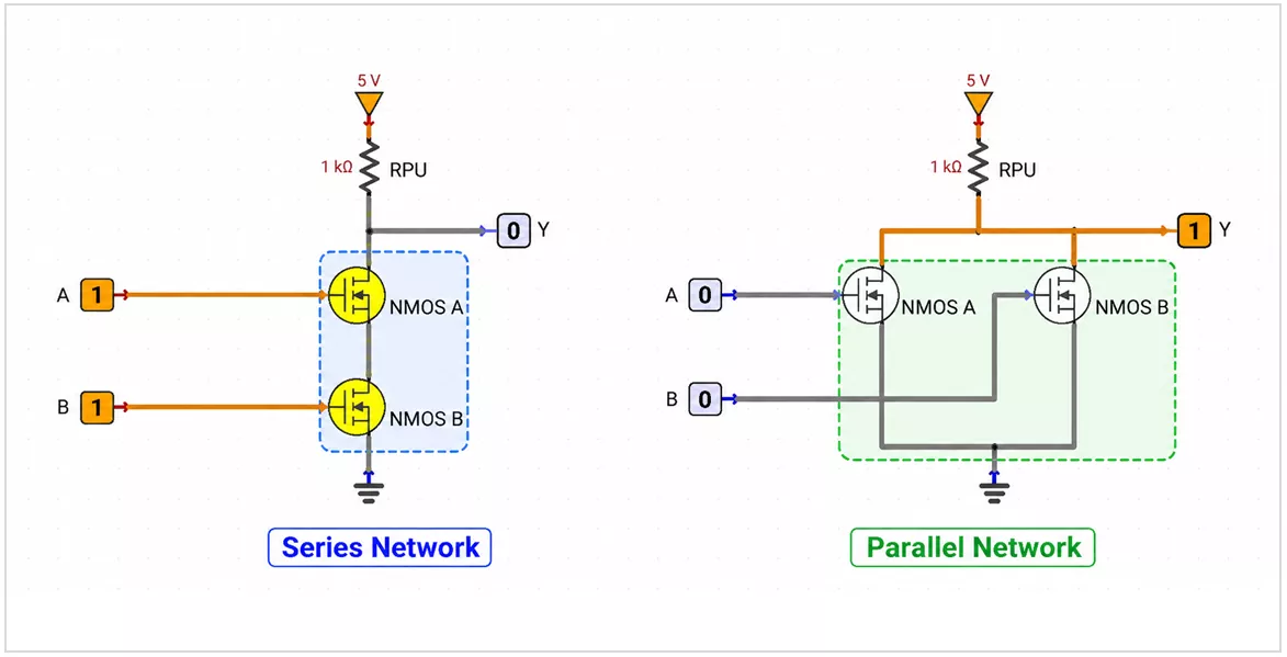
Series: all transistors must be ON. Parallel: any ON branch can complete the path.
For resistor-loaded pull-down logic:
- series NPN/NMOS → NAND behavior;
- parallel NPN/NMOS → NOR behavior.
CMOS uses a complementary pull-up network with the opposite series/parallel arrangement.
Basic Transistor Logic Gates
NOT Gate
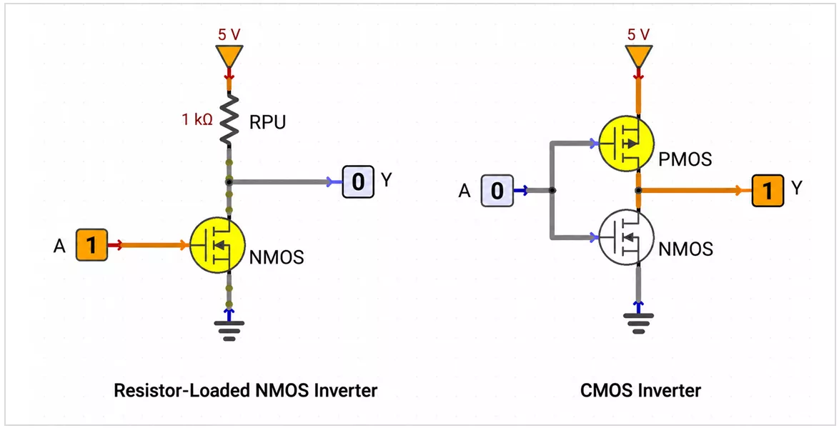
Y = A'NMOS inverter: A = 0 turns the NMOS OFF and the resistor pulls Y=HIGH; A = 1 turns the NMOS ON and pulls Y=LOW. CMOS uses complementary PMOS pull-up and NMOS pull-down devices.
NAND Gate
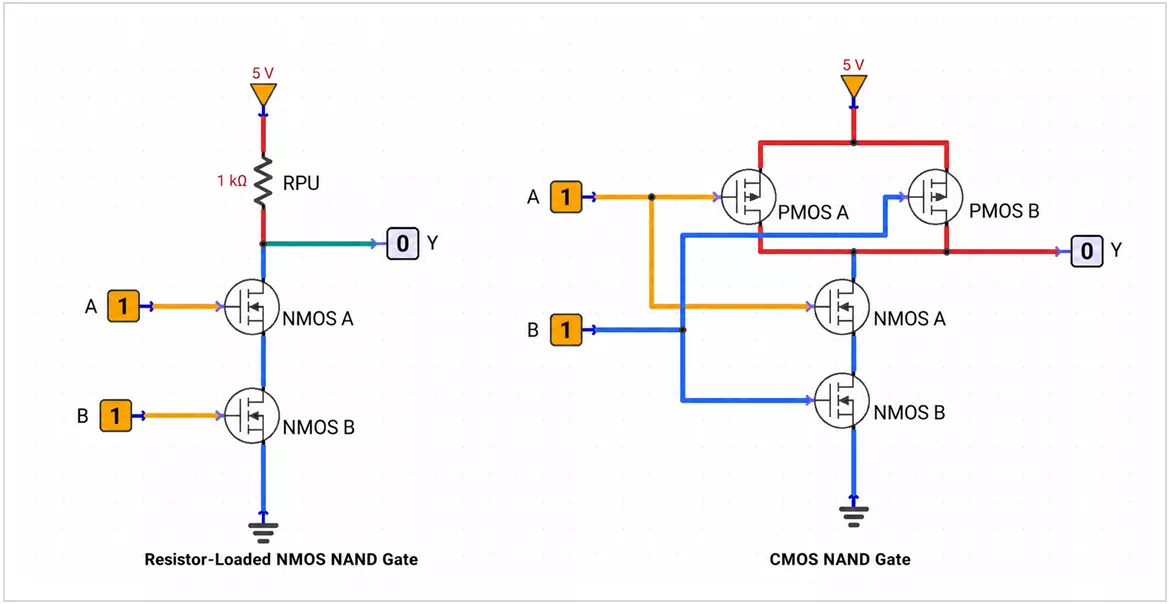
Y = (A · B)'Resistor-loaded NMOS NAND uses two NMOS transistors in series. CMOS NAND uses parallel PMOS devices in the pull-up network and series NMOS devices in the pull-down network.
NOR Gate
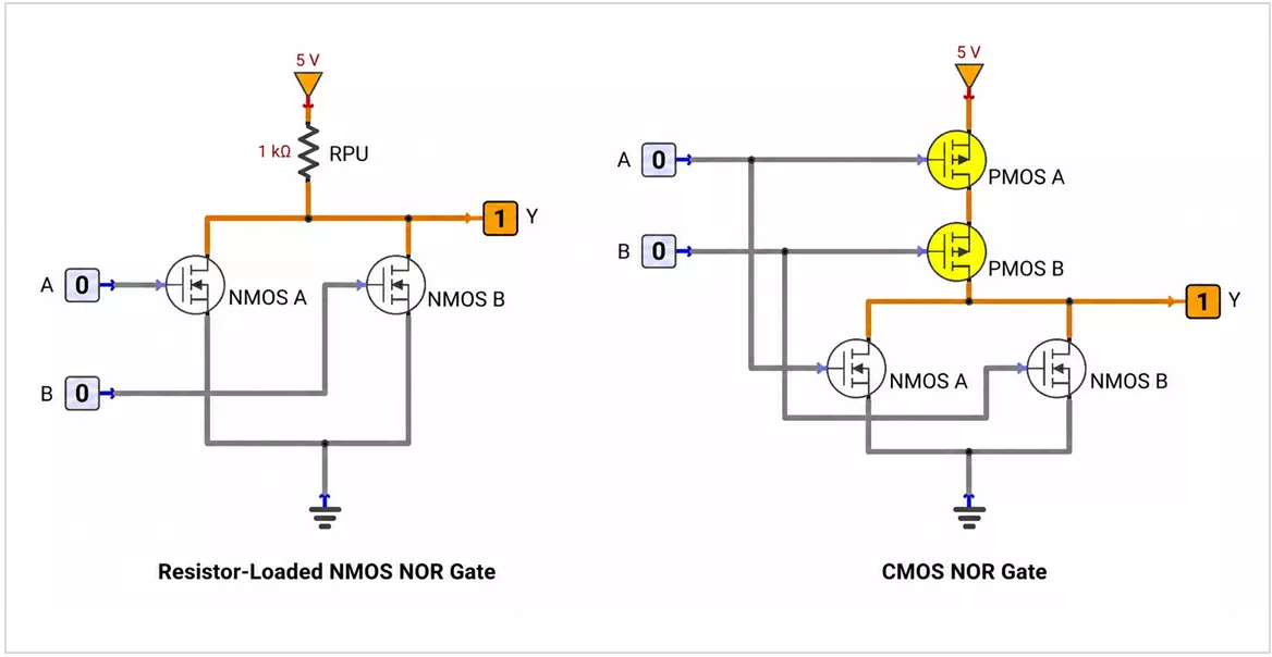
Y = (A + B)'Resistor-loaded NMOS NOR uses parallel NMOS pull-down branches. CMOS NOR uses series PMOS devices in the pull-up network and parallel NMOS devices in the pull-down network.
Derived Logic Gates
AND Gate
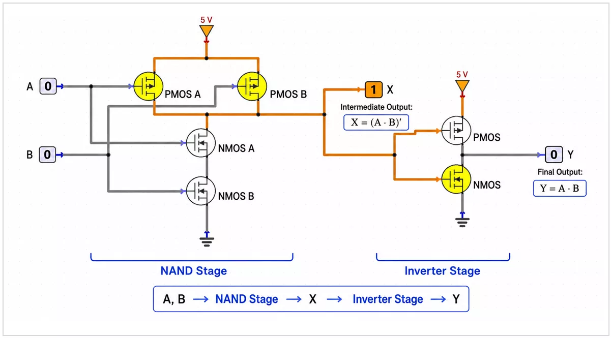
X = (A · B)' → Y = X' = A · BA NAND stage followed by an inverter produces AND.
OR Gate
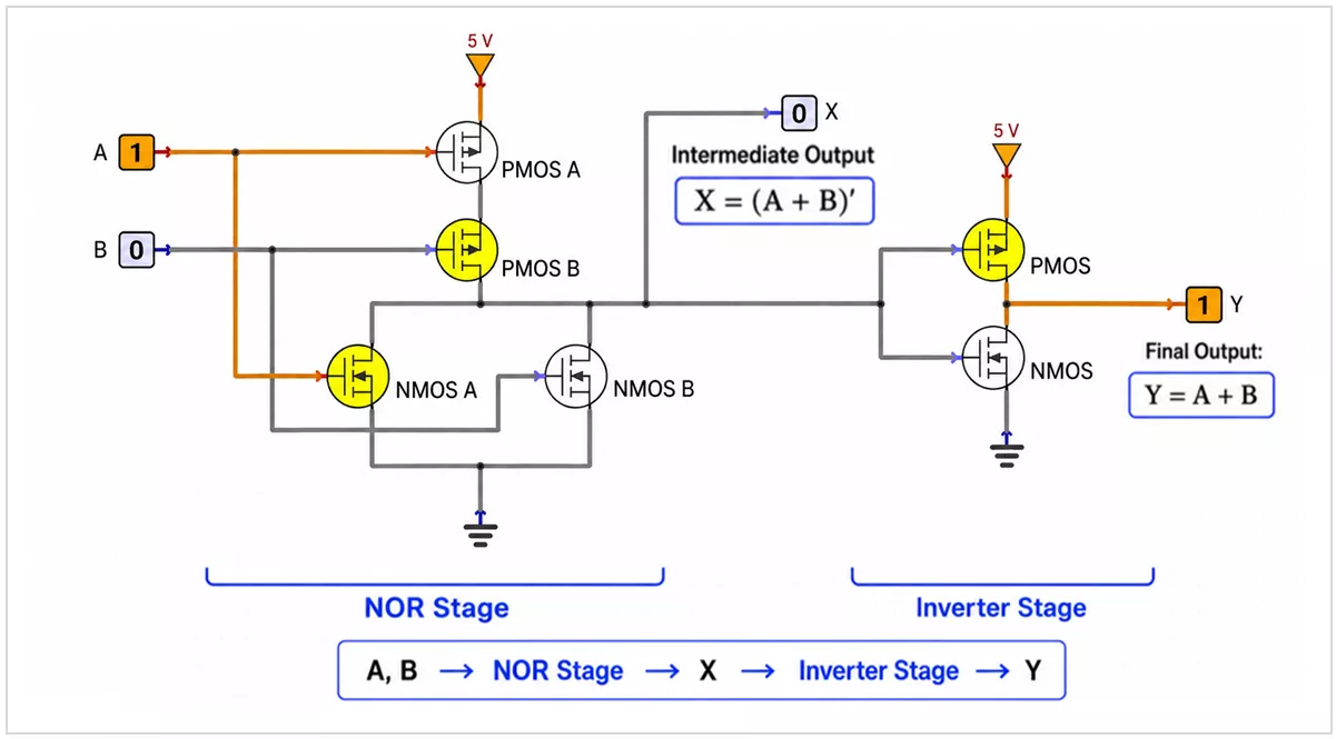
X = (A + B)' → Y = X' = A + BA NOR stage followed by an inverter produces OR.
Exclusive Logic Gates
XOR Gate
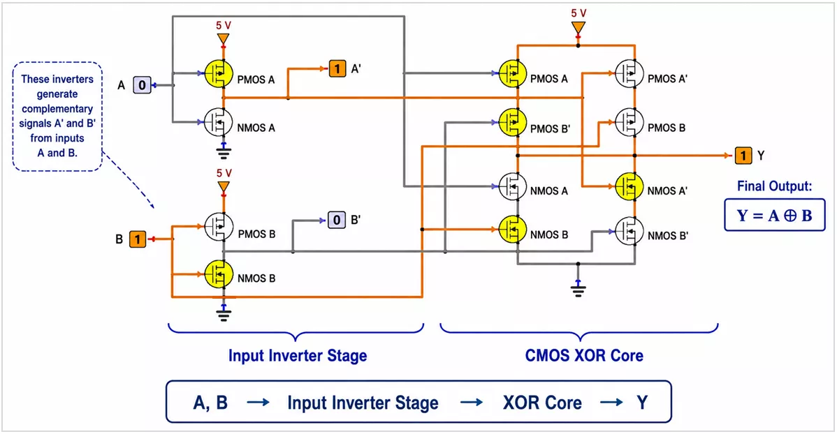
Y = A ⊕ B = A' · B + A · B'XOR is HIGH when the inputs are different. The shown static CMOS circuit first generates A' and B', then uses complementary pull-up and pull-down paths in the XOR core.
XNOR Gate
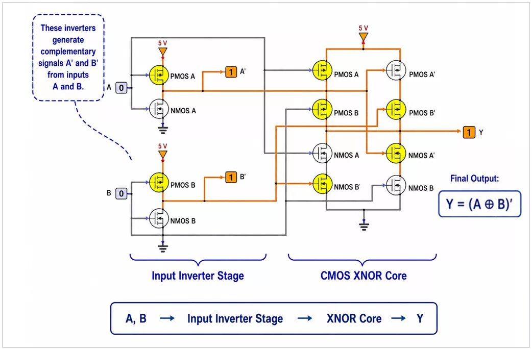
Y = (A ⊕ B)' = A · B + A' · B'XNOR is HIGH when the inputs are equal. It can be implemented as a complementary CMOS network or by inverting an XOR output.
Transistor Logic Families
The same Boolean function can be implemented using different transistor logic families.
| Logic Family | Devices Used | Basic Principle |
|---|---|---|
| RTL | BJTs + resistors | BJT switching with resistive load |
| TTL | BJTs | Multiple BJT stages perform logic and active output driving |
| MOS Logic | NMOS or PMOS + load | One MOSFET type forms the switching network |
| CMOS | NMOS + PMOS | Complementary pull-up and pull-down networks |
RTL Example
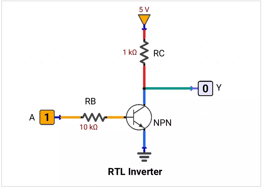
In a simple NPN RTL inverter, the resistor pulls Y HIGH when the transistor is OFF, while the NPN transistor pulls Y LOW when it turns ON.
TTL Example
TTL uses BJTs for both logic processing and active output driving. The shown teaching circuit uses separate input transistors Q1A and Q1B, a phase-splitter Q2, and a totem-pole output stage Q3–Q4.
- If A = 0 or B = 0, the pull-down output path is not activated and the output is driven HIGH.
- If A = 1 and B = 1, Q2 drives the pull-down transistor ON and the output becomes LOW.
Y = (A · B)'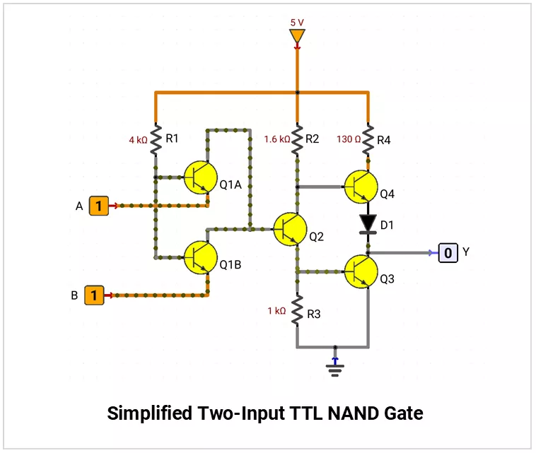
Note: Classic TTL NAND gates normally use a multi-emitter input transistor. This simplified teaching circuit uses separate input transistors to represent the input stage.