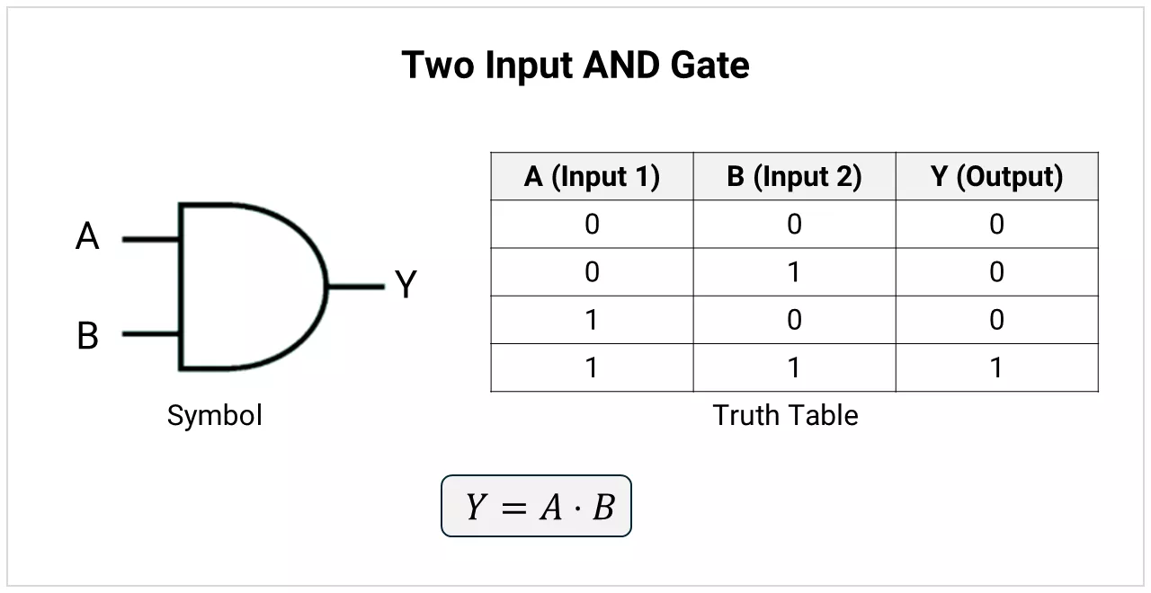
Design a circuit verifying a 2-input AND gate.
Constraints:
Behavioral Reference:
| A | B | Y |
|---|---|---|
| 0 | 0 | 0 |
| 0 | 1 | 0 |
| 1 | 0 | 0 |
| 1 | 1 | 1 |
Logic gate is a combinational circuit that combines binary inputs to produce a binary output. Its output depends on the present input values, changing after the circuit's propagation delay; it does not store a previous state.
Logic synthesis is the process of converting a required behaviour into a Boolean expression and implementing that expression with the permitted gates.
Basic design flow:
Requirement → Truth Table or Conditions → Boolean expression → Simplification → Gate circuit → Verification
1 represents HIGH and 0 represents LOW. A truth table lists the output for every possible input combination.
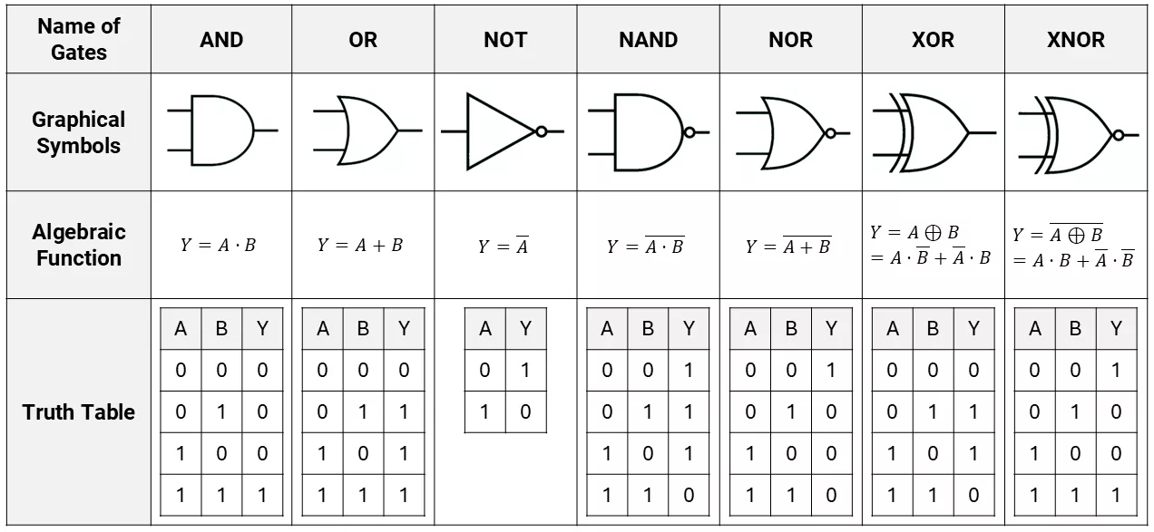
Table 1: Two-Input Gate Behaviour
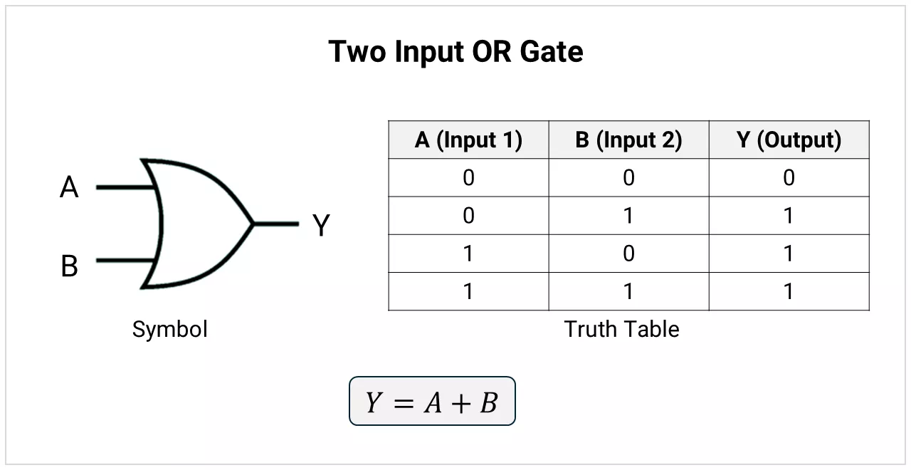
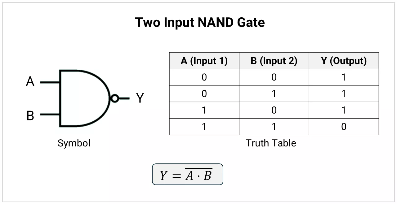
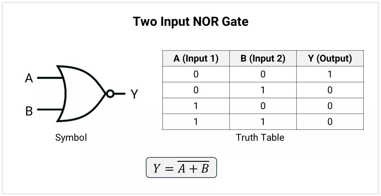
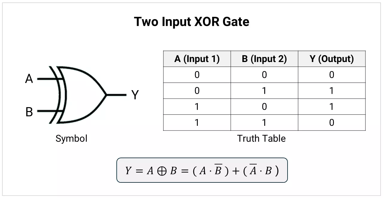
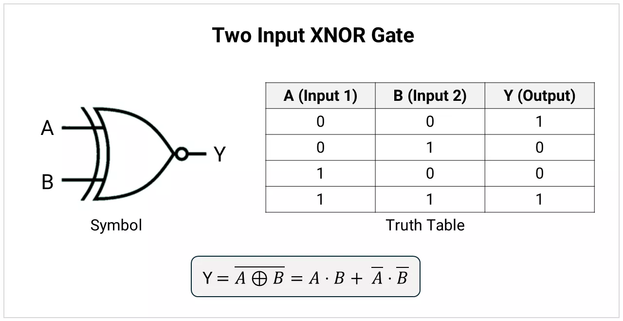
| Input A | Input B | AND | OR | NAND | NOR | XOR | XNOR |
|---|---|---|---|---|---|---|---|
| 0 | 0 | 0 | 0 | 1 | 1 | 0 | 1 |
| 0 | 1 | 0 | 1 | 1 | 0 | 1 | 0 |
| 1 | 0 | 0 | 1 | 1 | 0 | 1 | 0 |
| 1 | 1 | 1 | 1 | 0 | 0 | 0 | 1 |
| Gate | Output is HIGH when... |
|---|---|
| AND | Every input is HIGH |
| OR | At least one input is HIGH |
| NOT | The input is LOW |
| NAND | The AND result is LOW |
| NOR | Every input is LOW |
| XOR | The inputs are different |
| XNOR | The inputs are equal |
Before selecting gates, convert the written requirement into clear binary conditions.
Design method
1. List every input and output.
2. Decide what 0 and 1 mean for each signal.
3. Mark active-HIGH and active-LOW inputs.
4. Identify the conditions that must make the output HIGH.
5. Use AND for conditions required together, OR for alternative paths, NOT for an active-LOW condition, and XOR for an exactly-one or difference condition.
6. Write a truth table or test cases before building the circuit.
| Requirement pattern | Typical expression | Meaning |
| All conditions must be true | A·B·C | Output is HIGH only when every condition is HIGH |
| Any condition can activate the output | A+B+C | One or more conditions can make the output HIGH |
| An active-LOW condition must be inactive | ~L | HIGH when the lockout or fault signal is LOW |
| Enable a request | E·R | The request works only when enabled |
| Exactly one input is HIGH | A⊕B | One input is HIGH, but not both |
| Add an override path | Normal + Override | Either path can activate the output |
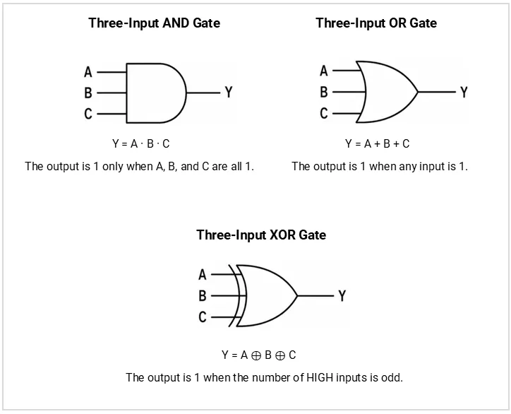
When a required gate has more inputs than the available gate, divide the operation into smaller stages and name the intermediate nodes.
Example: three-input AND using two-input gates
N1 = A·B
Y = N1·C = A·B·C
The same method applies to an OR function:
N1 = A+B
Y = N1+C = A+B+C
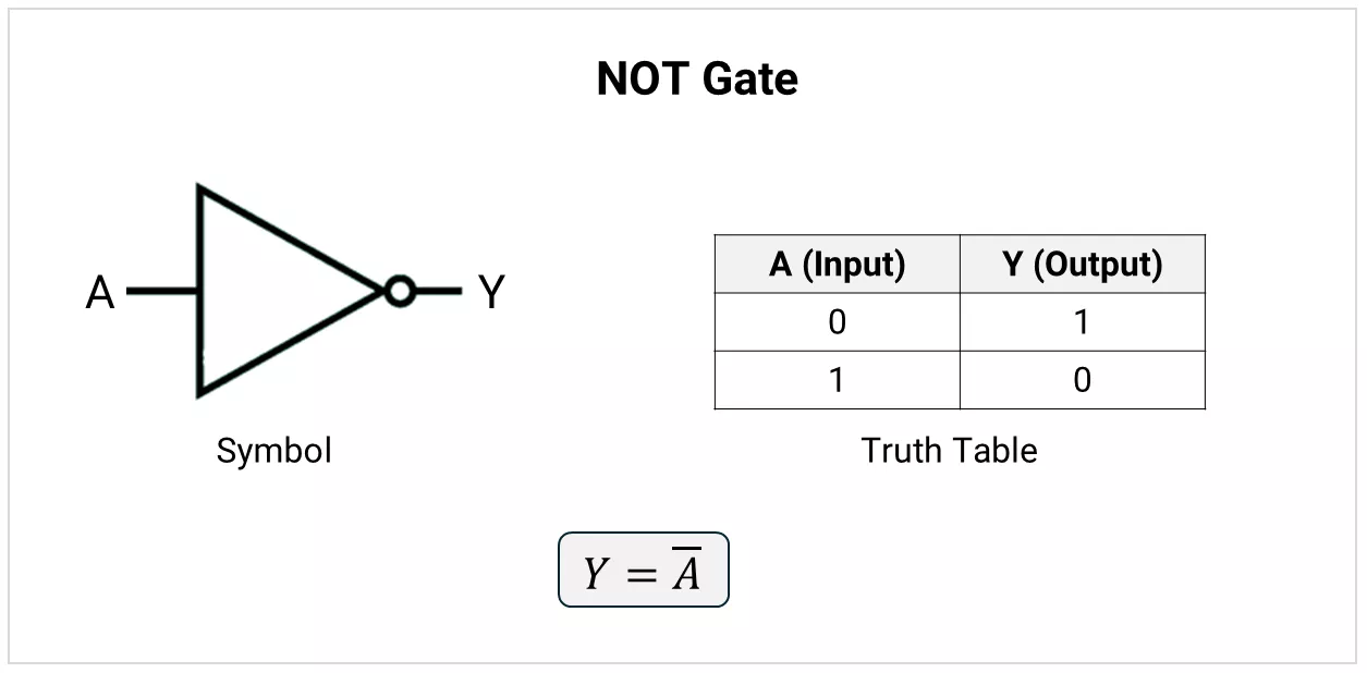
The symbol ~ means NOT or complement:
Y = ~A
Therefore, A=0 produces Y=1, and A=1 produces Y=0.
| Signal condition | Boolean form | Interpretation |
| Active-HIGH request | R | Asserted when R=1 |
| Active-LOW lockout | ~L | Operation is allowed when L=0 |
| Active-LOW sensor condition | ~S | The physical condition is represented by S=0 |
| Inverted output | ~Y | Reverses the output polarity |
An inversion can appear as a NOT gate, a bubble on a gate symbol, an active-LOW pin label, or a complemented term in an equation. Include it at the correct point in the signal path.
XOR detects a difference. XNOR detects equality.
Table 2: XOR and XNOR Operation
| A | B | XOR | XNOR | Interpretation |
|---|---|---|---|---|
| 0 | 0 | 0 | 1 | Equal |
| 0 | 1 | 1 | 0 | Different |
| 1 | 0 | 1 | 0 | Different |
| 1 | 1 | 0 | 1 | Equal |
Read a combinational circuit from the inputs toward the output.
Analysis method
1. Name each intermediate node.
2. Write one equation for every gate.
3. Substitute the intermediate equations into the output equation.
4. Check all inversions and gate polarities.
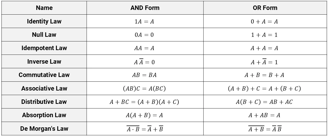
5. Simplify the expression and verify it with a truth table or a few distinguishing input combinations.
Table 3: Common Boolean Laws
| Boolean law | Form | Typical use |
| De Morgan | ~(A·B) = ~A + ~B | convert NAND-style logic to OR-style logic |
| De Morgan | ~(A+B) = ~A·~B | convert NOR-style logic to AND-style logic |
| Distributive | A·B + A·C = A·(B+C) | factor a common term |
| Complement | A+~A=1, A·~A=0 | remove impossible or always-true conditions |
| Absorption | A + A·B = A | remove a redundant path |
| Identity | A+0=A, A·1=A | remove neutral inputs |
Generic reduction
· F = X·Y + X·Z
· F = X·(Y+Z)
The factored expression may use fewer gates or less duplicated logic, but the allowed gate types, fan-in, and propagation delay must still be checked.
Restricted synthesis means implementing the required function without using one or more convenient gate types.
Design method
1. Write the required Boolean function.
2. List the allowed and prohibited gates.
3. Apply Boolean identities to match the allowed set.
4. Replace each operation with an allowed gate connection.
5. Check the output polarity of every intermediate node.
6. Verify the final truth table, gate count, and gate depth.
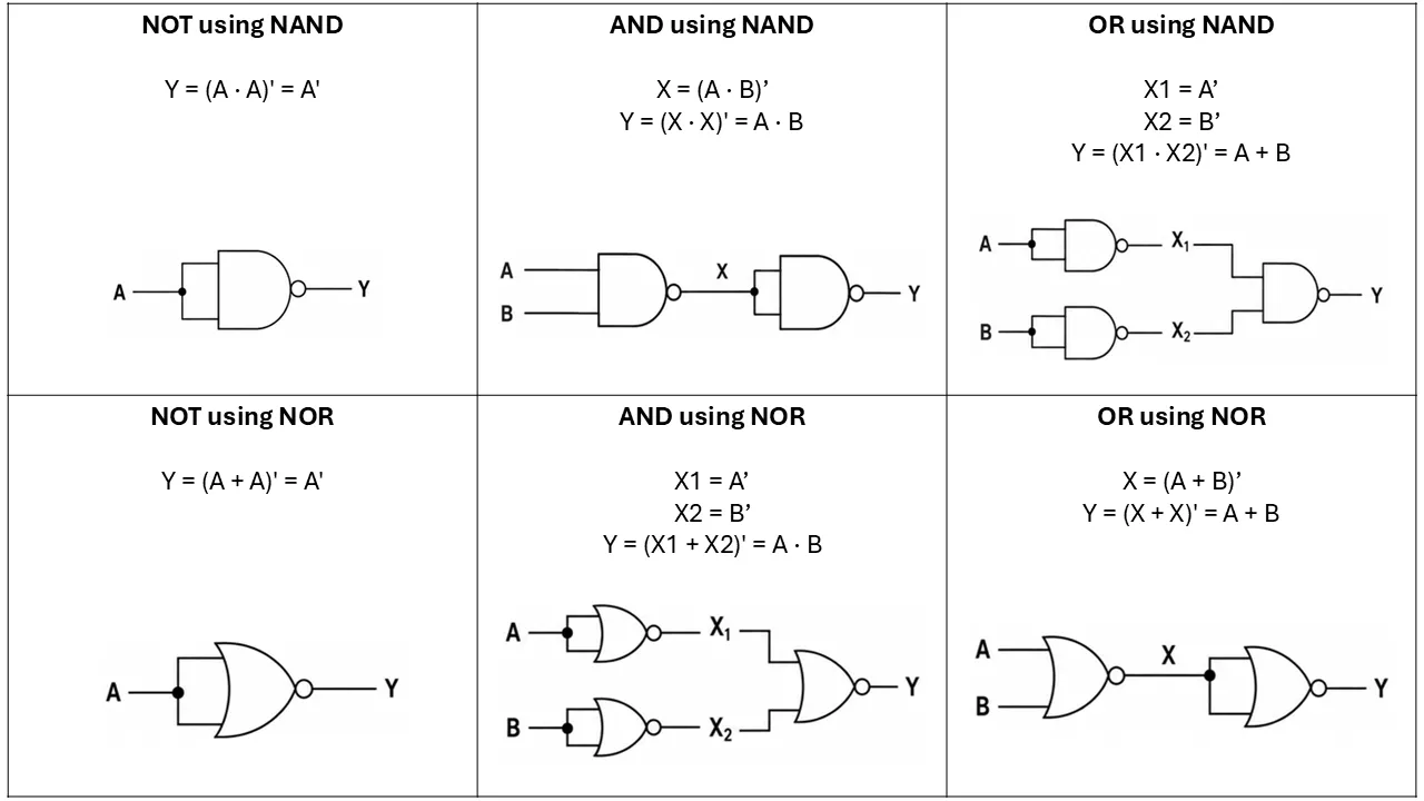
NAND and NOR are universal gates because suitable connections can create NOT, AND, OR, and larger combinational functions.
Table 4: Basic Universal-Gate Conversions
| Required function | NAND-only form | NOR-only form |
| NOT ~A | ~(A·A) | ~(A+A) |
| AND A·B | ~(~(A·B)·~(A·B)) | ~(~(A+A)+~(B+B)) |
| OR A+B | ~(~(A·A)·~(B·B)) | ~(~(A+B)+~(A+B)) |
Tying both inputs of a NAND or NOR gate to the same signal creates an inverter. The tied-input gate still counts as one physical gate and adds a logic level.
Reusable NAND pattern: sum of two product terms
The final NAND performs the required OR through De Morgan's theorem. This pattern can be extended to more product terms by using a suitable NAND tree.
Boolean identities can convert a target function into a form using the available gates.
| Target operation | Example identity |
| AND using OR and XOR | A·B = (A+B) ⊕ (A⊕B) |
| OR using AND and XOR | A+B = (A·B) ⊕ (A⊕B) |
| Inversion using a tied-input NAND | ~A = ~(A·A) |
| Inversion using a tied-input NOR | ~A = ~(A+A) |
| Inversion using XOR and HIGH | ~A = A⊕1 |
Do not assume that a gate's name describes the polarity of its output. Write the equation of the gate actually used, then simplify it.
Propagation delay is the time between an input change and the corresponding output change. The critical path is the longest input-to-output path.
For equal gate delays:
Critical-path delay = number of gate levels on the longest path · delay per gate
Table 6: Structural Effects on a Combinational Circuit
| Circuit feature | Effect |
| Gates in series | delays add |
| Independent parallel branches | only the longest branch matters before the next common gate |
| Balanced gate tree | can reduce the number of levels |
| Factored expression | may reduce duplicated logic and hardware |
| More gates in parallel | does not automatically mean a longer critical path |
When comparing equivalent implementations, evaluate both resource use and logic depth. Fewer total gates do not always mean a faster circuit if the longest path is deeper.
If multiple outputs use the same complete product term or intermediate expression, generate it once and fan it out where the circuit technology allows. Sharing reduces hardware, but added fan-out can affect delay.
For a suspected combinational fault, compare the expected behaviour with the observed behaviour at the internal nodes and final output.
Fault-analysis method
1. Write the expected equation or truth-table result.
2. Identify the suspected gate, connection, or internal node.
3. Choose a sensitizing input—an input combination that makes the node's value affect the output rather than masking it.
4. Propagate the correct and faulty values through the remaining gates.
5. Compare the expected and observed output.
| Suspected fault | Useful test condition |
| Node stuck at 0 | choose inputs for which the node should be 1 |
| Node stuck at 1 | choose inputs for which the node should be 0 |
| Wrong inversion | test both active and inactive input conditions |
| Wrong gate type | test an input combination where the two candidate gates differ |
| Missing connection | activate the missing path while holding unrelated inputs inactive |
One input combination with different outputs proves that two implementations are not equivalent. To establish equivalence, compare their truth tables or simplify both expressions to the same form.
Always check inversion bubbles, active-LOW signals, intermediate nodes, and the conditions required to make a fault observable.
Before finalising a logic-gate or synthesis circuit, check: