72. Design 4-bit left shift register using D FF
Implement a 4-bit synchronous Left Shift Register using four positive-edge-triggered D Flip-Flops connected in series.
Constraints:
- On each rising Clock edge, shift data left:
D → Q0,Q0 → Q1,Q1 → Q2,Q2 → Q3. - Connect outputs Q3, Q2, Q1, and Q0 to provided 4-bit output bus "Q3_Q2_Q1_Q0".
- Hold the current state when there is no rising clock edge.
Behaviour reference:
| D | CLK | Q3+ | Q2+ | Q1+ | Q0+ |
|---|---|---|---|---|---|
| X | ↓ | Q3 | Q2 | Q1 | Q0 |
| 1 | ↑ | 0 | 0 | 0 | 1 |
| 0 | ↑ | 0 | 0 | 1 | 0 |
| 1 | ↑ | 0 | 1 | 0 | 1 |
| 1 | ↑ | 1 | 0 | 1 | 1 |
| 0 | ↑ | 0 | 1 | 1 | 0 |
A register is a group of flip-flops used to store a binary value. Each flip-flop stores one bit.
2-bit Register:-
A 2-bit register uses two D flip-flops to store one 2-bit value.
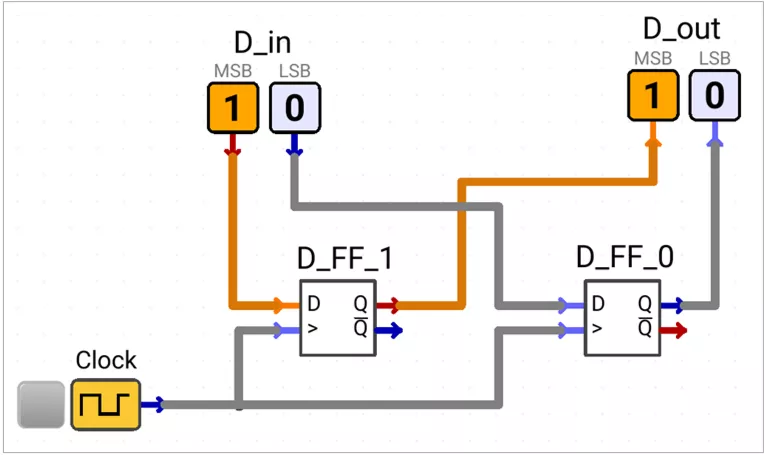
- D_FF_1 stores the most significant bit (MSB).
- D_FF_0 stores the least significant bit (LSB).
- Both bits are stored together at the rising edge of the clock.
Right Shift Register
A right shift register moves each stored bit from MSB to LSB at every active clock edge.
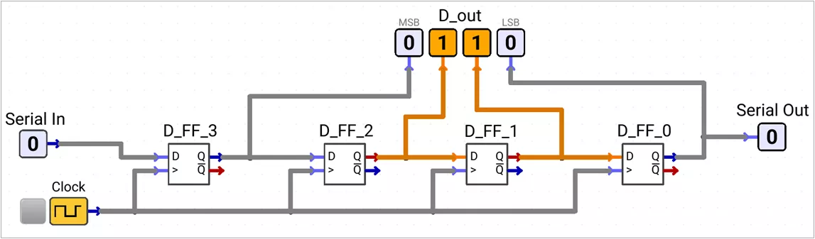
Serial In → Q3 → Q2 → Q1 → Q0 → Serial Out- Serial data enters at Q3 (MSB) from Serial In.
- Data leaves the register from Q0, the LSB.
Left Shift Register
A left shift register moves each stored bit from LSB to MSB at every active clock edge.
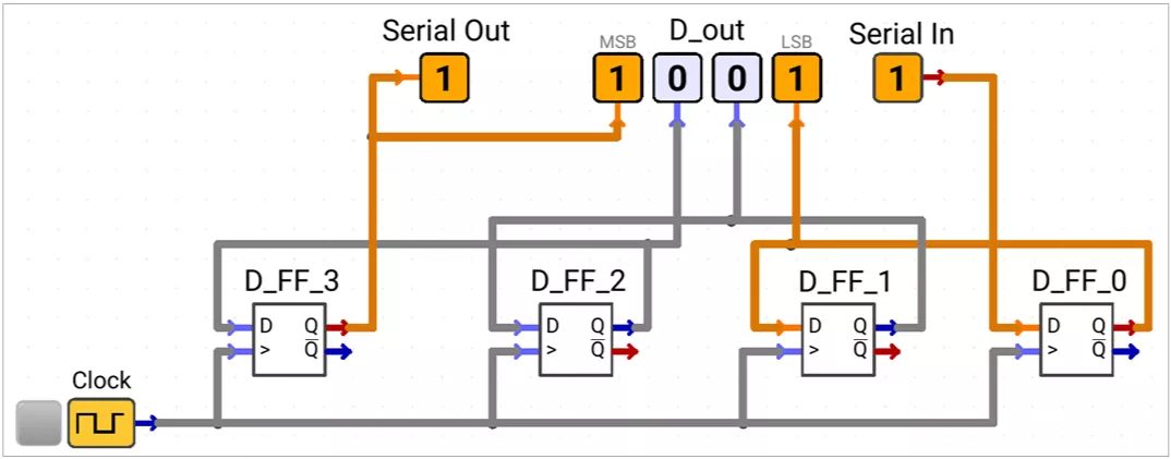
Serial In → Q0 → Q1 → Q2 → Q3 → Serial Out- Serial data enters at Q0 (LSB) from Serial In.
- Data leaves the register from Q3, the MSB.
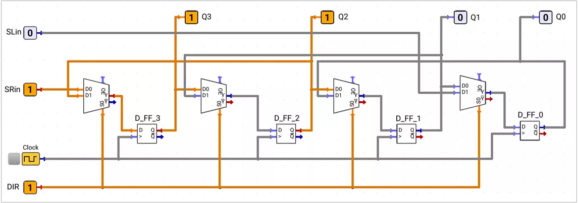
Bi-directional Shift Register
A bi-directional shift register moves data in either direction.
DIR = 0: selects right shift.DIR = 1: selects left shift.
DIR = 0: Right Shift | DIR = 1: Left Shift | Flip-Flop input |
|---|---|---|
SRin | Q2 | D3 |
Q3 | Q1 | D2 |
Q2 | Q0 | D1 |
Q1 | SLin | D0 |
SRinis the right-shift serial input.SLinis the left-shift serial input.
Edge Detector Circuit
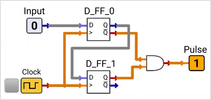
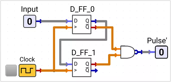
An edge detector is a sequential circuit that activates when the required input transition appears.
- Two D flip-flops store the current and previous input samples.
- Q0 is the current sampled input.
- Q1 is the previous sampled input.
- An AND gate gives an active-HIGH pulse.
- A NAND gate gives an active-LOW pulse.
Rising-edge active-HIGH = Q0 · Q₁’
Falling-edge active-HIGH = Q₀’· Q1| Rising Edge (0 → 1) | Falling Edge (1 → 0) | |
|---|---|---|
Active-HIGH output pulse Idle: 0 Active: 1 | 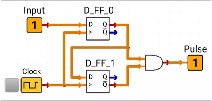
| 
|
Active-LOW output pulse Idle: 1 Active: 0 | 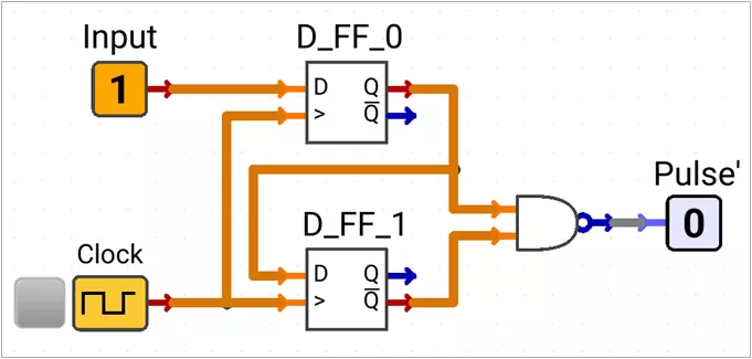
| 
|
Applications
- Push-button press detection.
- Single-clock pulse generation.
- Counter or register enable control.
- Event and interrupt detection.
Digital Data Transmission
Shift registers convert and transmit data in serial or parallel form.
| Type | Input method | Output method | Application |
|---|---|---|---|
PIPO | Parallel | Parallel | Data storage or bus buffer |
SISO | Serial | Serial | Digital delay line |
SIPO | Serial | Parallel | Serial data receiver |
PISO | Parallel | Serial | Serial data transmitter |
Parallel-In Parallel-Out (PIPO)
All input bits are loaded together and appear together at the outputs.
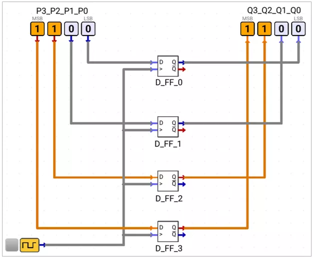
P3_P2_P1_P0 → Q3_Q2_Q1_Q0Serial-In Serial-Out (SISO)
Bits enter and leave one at a time. A 4-bit SISO delays the first bit by four active clock edges.
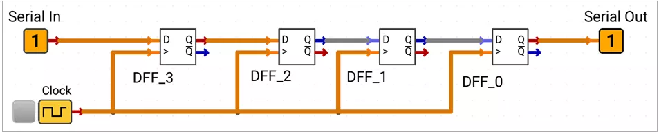
Serial In → Q3 → Q2 → Q1 → Q0 → Serial OutSerial-In Parallel-Out
Bits enter serially. After four active clock edges, the 4-bit word is available at Q3 to Q0.
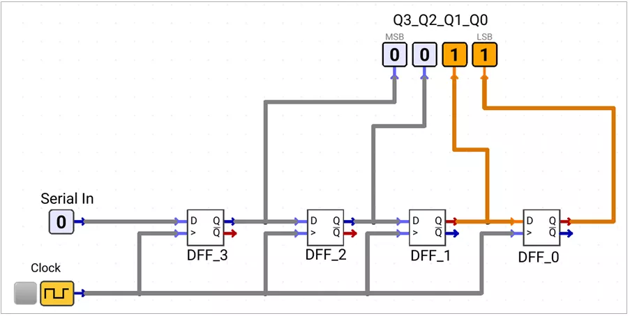
Serial In → Q3 → Q2 → Q1 → Q0Parallel-In Serial-Out
A PISO register loads a complete word and then shifts it out one bit at a time. It uses an additional LOAD input.
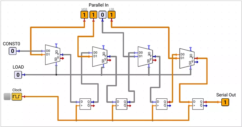
LOAD = 1: Parallel input data is loaded.LOAD = 0: Data is shifted towardSerial Out.
Parallel to Serial to Parallel Transmission
PISO → Transmission Line → SIPO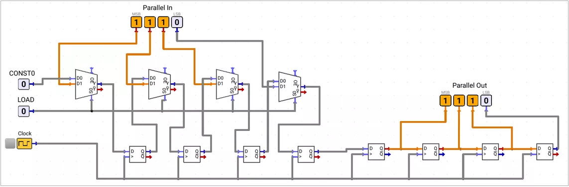
LOAD = 1: The PISO register loads the parallel data.LOAD = 0: The PISO register transmits one bit per active clock edge.- The SIPO register receives the bits and rebuilds the parallel word.
- A 4-bit word requires four active clock edges at the receiver.
Applications
- Communication between digital boards using fewer wires.
- Sensor or peripheral data transfer.
- Serial links between controllers and display drivers.
Register Applications:
LED Belt
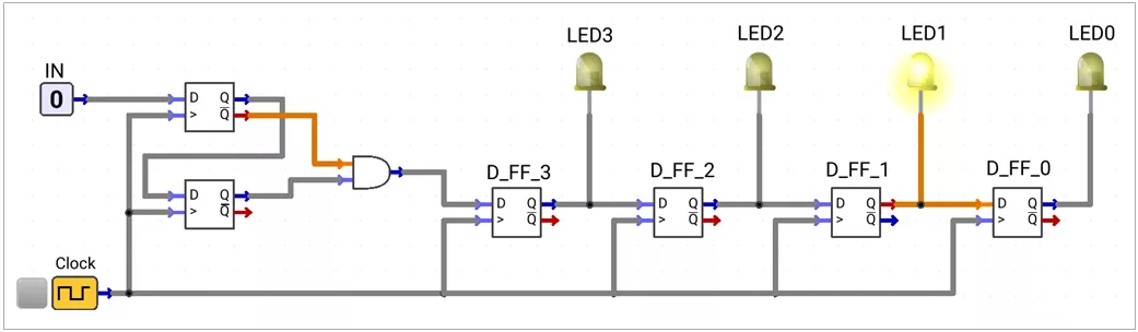
Circuit behaviour
- A sampled falling edge of
INgenerates a HIGH pulse, which is loaded intoQ3on the following active clock edge. - Each rising clock edge shifts it from Q3 to Q0, lighting one active-HIGH LED.
Functional table
| Clock event | IN | Q3 | Q2 | Q1 | Q0 | LED Glowing |
|---|---|---|---|---|---|---|
↑ | 1 | 0 | 0 | 0 | 0 | NONE |
↑ | 0 | 0 | 0 | 0 | 0 | NONE |
↑ | 0 | 1 | 0 | 0 | 0 | LED3 |
↑ | 0 | 0 | 1 | 0 | 0 | LED2 |
↑ | 0 | 0 | 0 | 1 | 0 | LED1 |
↑ | 0 | 0 | 0 | 0 | 1 | LED0 |
↑ = rising clock edge.
Digital Lock
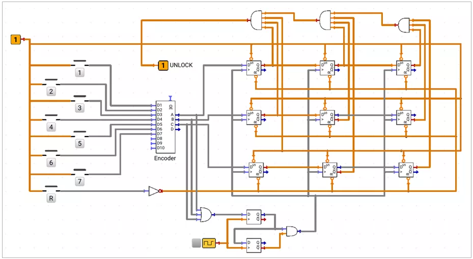
Implementation:
- Input selection:
- Buttons 1 to 7 drive D1 to D7 of a 10:4 encoder.
- Outputs A, B, and C form the 3-bit code; D is unused.
- Button press detection:
- When no button is pressed, the encoder outputs
0000. - Since only buttons 1–7 are used, every valid button code makes at least one of A, B, or C HIGH.
- Therefore,
(A + B + C)detects a button press using only a 3-input OR gate. - A rising-edge detector converts this signal into one short storage pulse.
- When no button is pressed, the encoder outputs
- Sequence storage:
- Three 3-bit PIPO stages store the last three button codes.
- Each new code advances the older codes by one stage.
- Code matching: Combinational AND logic checks the stored sequence
5, 1, 7.It setsUNLOCK = 1only for this sequence. - Reset:
Ris inverted before reaching the active-LOW CLR inputs. PressingRclears every PIPO stage.
Working
- Press 5, then 1, then 7.
- Each press creates one pulse and stores the encoded 3-bit value.
- After the third correct value, the matching logic sets
UNLOCK = 1. - A wrong sequence keeps
UNLOCK = 0. PressRto clear the stored sequence.
5 → 1 → 7 → UNLOCK = 1