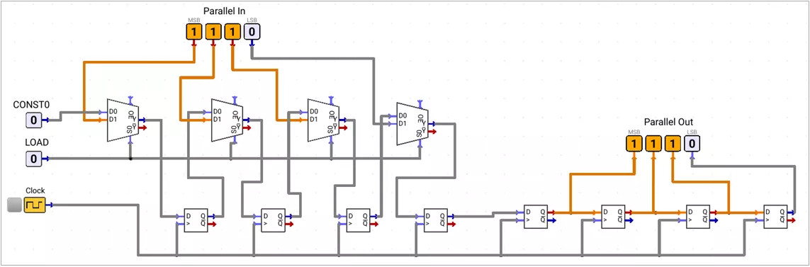
73. Design PISO register for custom UART Transmitter

Implement a 4-bit synchronous Parallel-In Serial-Out (PISO) shift register to emulate a basic UART Transmitter (Tx). The circuit should support parallel data loading and serial transmission under the control of a 1 Hz clock.

Constraints:

  • You have given a 4-bit parallel input bus (D_in), a control line (CTR), and a 1 Hz clock.
  • When CTR = 0, synchronously load the 4-bit parallel data into the register.
  • When CTR = 1, shift data out serially with the LSB transmitted first.
  • Shift data from Q3 → Q2 → Q1 → Q0, with Q0 serving as the serial output (D_out).
  • Ensure both loading and shifting occur only on the rising edge of the 1 Hz clock.

Behaviour reference:

Consider the input data as 1001

Clock pulseCTRQ3+Q2+Q1+Q0+
InitialX0000
1 (Rising Edge)01001
2 (Rising Edge)11100
3 (Rising Edge)11110
4 (Rising Edge)11111
5 (Rising Edge)11111
Need Help? Refer to the Quick Guide below

Basic Concept of Register

A register is a group of flip-flops used to store a binary value.

  • Each flip-flop stores 1 bit.
  • All flip-flops normally use a common clock.
  • An n-bit register requires n flip-flops.

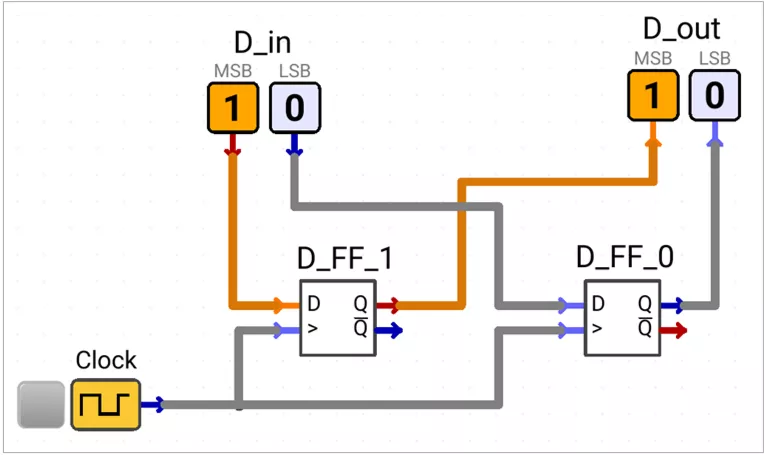
2-Bit Register Example

A 2-bit register contains two D flip-flops:

  • D1 stores the MSB.
  • D0 stores the LSB.
  • Outputs are Q1 and Q0.

Both flip-flops receive the same clock signal.

Fig. 1: 2-bit Register

two-bit-parallel-register

Working

  • Before the active clock edge, the register keeps its previous value.
  • At the active clock edge, D1D0 is stored in Q1Q0.
  • The stored value remains unchanged until the next active clock edge.

Table 1: 2-Bit Register Example

ConditionD1D0Q1Q0
Before clock edge10Previous value
At active clock edge1010
After clock edgeX10

X means the input value does not affect the already stored output.


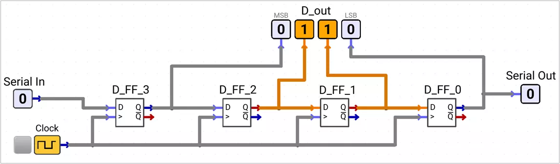
Right Shift Register

A right shift register moves every stored bit one position toward the LSB.

For a 4-bit register:

Q3 → Q2 → Q1 → Q0

Here:

  • Q3 is the MSB.
  • Q0 is the LSB.
  • New serial data enters Q3.
  • Data leaves from Q0.

Fig. 2: 4-bit Right Shift Register

four-bit-right-shift-register

Connections

  • D3 = Serial In
  • D2 = Q3
  • D1 = Q2
  • D0 = Q1
  • Serial Out = Q0

Working

At every active clock edge:

  • Q3 receives the serial input.
  • Q2 receives the previous Q3.
  • Q1 receives the previous Q2.
  • Q0 receives the previous Q1.

Table 2: Right Shift Example

Present ValueSerial InputValue After Clock
101100101

The bits move from MSB to LSB.


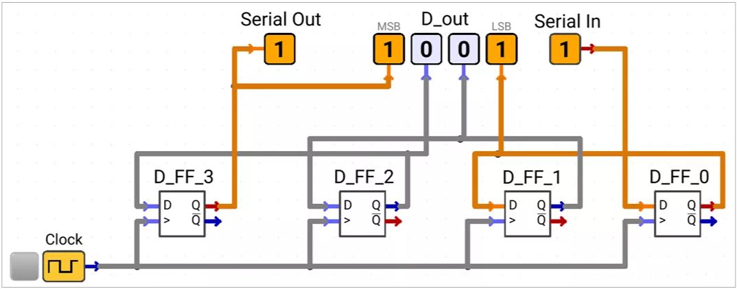
Left Shift Register

A left shift register moves every stored bit one position toward the MSB.

For a 4-bit register:

Q0 → Q1 → Q2 → Q3

Here:

  • New serial data enters Q0.
  • Data leaves from Q3.

Fig. 3: 4-bit Left Shift Register

four-bit-left-shift-register

Connections

  • D0 = Serial In
  • D1 = Q0
  • D2 = Q1
  • D3 = Q2
  • Serial Out = Q3

Working

At every active clock edge:

  • Q0 receives the serial input.
  • Q1 receives the previous Q0.
  • Q2 receives the previous Q1.
  • Q3 receives the previous Q2.

Table 3: Left Shift Example

Present ValueSerial InputValue After Clock
101100110

The bits move from LSB to MSB.


Edge Detector Circuit

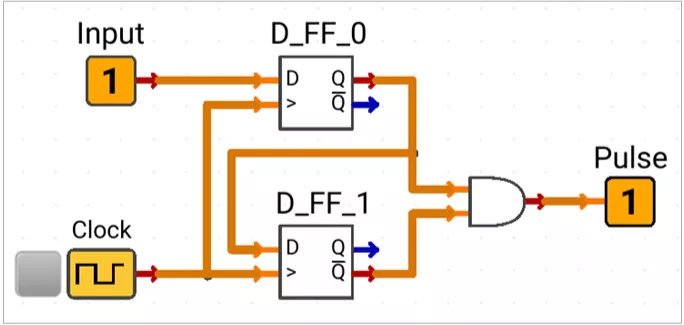
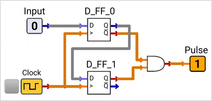
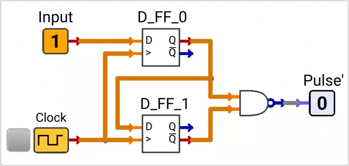
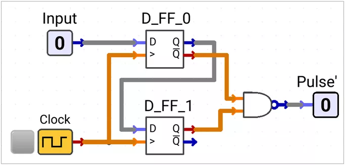
An edge detector produces a short pulse when an input signal changes from one logic level to another.

It uses two clocked samples:

  • Q0 – current sampled input
  • Q1 – previous sampled input

The output pulse normally remains active for one clock cycle.

Table 4: Edge Detector Types

 Rising Edge 0 → 1Falling Edge 1 → 0
Active-HIGH output
active-high-rising-edge-detector

The output becomes 1 for one clock cycle when the input changes from 0 to 1.

active-high-falling-edge-detector

The output becomes 1 for one clock cycle when the input changes from 1 to 0.

Active-LOW output
active-low-rising-edge-detector

The output becomes 0 for one clock cycle when the input changes from 0 to 1.

active-low-falling-edge-detector

The output becomes 0 for one clock cycle when the input changes from 1 to 0.

Applications

  • Detecting push-button presses
  • Generating counter pulses
  • Capturing data in registers
  • Starting serial data transmission
  • Detecting changes in control signals
  • Generating one-clock enable pulses


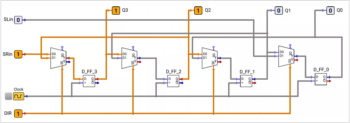
Bi-Directional Shift Register

A bi-directional shift register can shift data in both directions.

  • Right shift: MSB to LSB
  • Left shift: LSB to MSB

A direction input DIR selects the shifting direction.

Fig. 4: 4-bit Bi-directional Shift Register with Two inputs

four-bit-bidirectional-shift-register

Circuit Structure

Each flip-flop input is connected to a 2-to-1 multiplexer.

The multiplexer selects:

  • Data from the left-side flip-flop for right shifting
  • Data from the right-side flip-flop for left shifting

Two serial inputs are used:

  • SRin – enters the MSB during right shift
  • SLin – enters the LSB during left shift

Table 5: Bi-Directional Register Connections

Flip-Flop InputDIR = 0 Right ShiftDIR = 1 Left Shift
D3SRinQ2
D2Q3Q1
D1Q2Q0
D0Q1SLin

Working

When DIR = 0

  • The multiplexers select the right-shift connections.
  • Data moves from Q3 toward Q0.
  • New data enters through SRin.

When DIR = 1

  • The multiplexers select the left-shift connections.
  • Data moves from Q0 toward Q3.
  • New data enters through SLin.

The selected shift occurs at every active clock edge.


Register Input and Output Types

Registers are classified by how data enters and leaves them.

Table 6: Register Type Comparison

TypeInput MethodOutput MethodMain Function
PIPOParallelParallelStore a complete binary word
SISOSerialSerialShift or delay serial data
SIPOSerialParallelConvert serial data to parallel
PISOParallelSerialConvert parallel data to serial


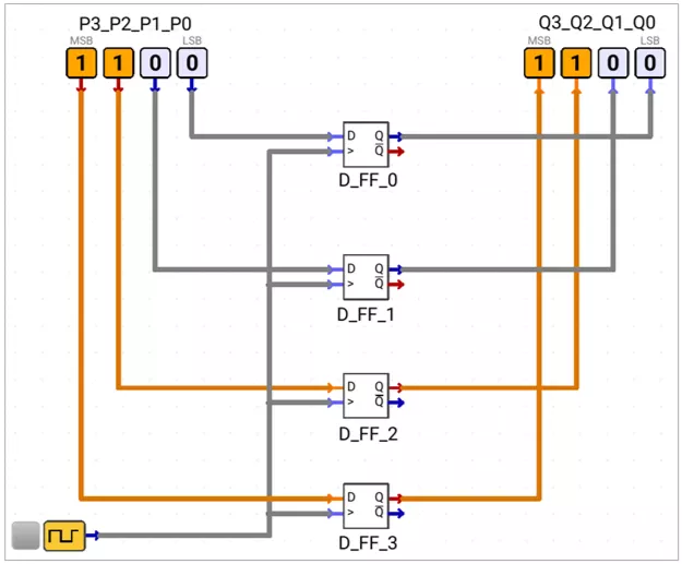
PIPO Register

PIPO means Parallel-In Parallel-Out.

All input bits are loaded together, and all output bits are available together.

Fig. 5: Parallel-in Parallel-out Shift Register

pipo-register-circuit

Connections

  • Each parallel input is connected to one D flip-flop.
  • All flip-flops share a common clock.
  • Each flip-flop provides a separate output.

Working

At the active clock edge:

Q3Q2Q1Q0 = P3P2P1P0

The complete binary word is stored in one clock operation.

Functionality

  • Temporary data storage
  • Data buffering
  • Processor registers
  • Parallel data transfer


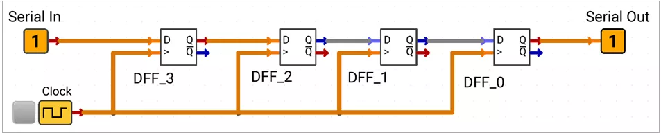
SISO Register

SISO means Serial-In Serial-Out.

Data enters one bit at a time and leaves one bit at a time.

Fig. 6: Serial-in Serial-out Shift Register

siso-register-circuit

Connections

  • The output of each flip-flop connects to the input of the next flip-flop.
  • The first flip-flop receives the serial input.
  • The last flip-flop provides the serial output.

Working

At each active clock edge:

  • One new bit enters the register.
  • Every stored bit moves one position.
  • One bit leaves through the serial output.

For an n-bit SISO register, a bit reaches the output after n clock edges.

Functionality

  • Serial data delay
  • Digital delay lines
  • Bit-by-bit data transfer


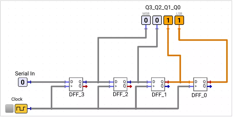
SIPO Register

SIPO means Serial-In Parallel-Out.

Data enters one bit at a time, but all stored bits can be read together.

Fig. 7: Serial-in Parallel-out Shift Register

sipo-register-circuit

Connections

  • The flip-flops are connected as a serial shift register.
  • Each flip-flop output is also available as a parallel output.

Working

  • One serial bit enters during each clock edge.
  • The bits move through the register.
  • After the required number of clock edges, the complete word is available at the parallel outputs.

Functionality

  • Serial-to-parallel conversion
  • LED control
  • Expanding processor output pins
  • Receiving serial data


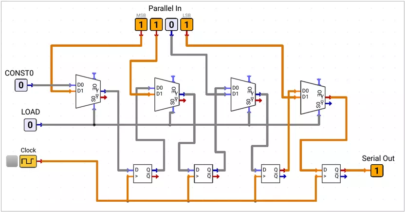
PISO Register

PISO means Parallel-In Serial-Out.

A complete binary word is loaded together and then shifted out one bit at a time.

Fig. 8: Parallel-in Serial-out Shift Register

piso-register-circuit

Connections

Each flip-flop uses a multiplexer to select:

  • Parallel input during load
  • Previous flip-flop output during shift

A LOAD input controls the operation.

Working

When LOAD = 1

All parallel input bits are loaded together:

Q3Q2Q1Q0 = P3P2P1P0

When LOAD = 0

The stored data shifts one bit during each clock edge.

For right shifting:

  • Data moves toward Q0.
  • Serial data leaves from Q0.

Functionality

  • Parallel-to-serial conversion
  • Sending processor data over one wire
  • Serial communication
  • Reducing transmission wires


Parallel-to-Serial-to-Parallel Transmission

Parallel data can be transmitted through one serial line using:

PISO → Transmission Line → SIPO

Fig. 9: Parallel to Serial to Parallel Transmission

parallel-serial-parallel-data-transmission

Working

  1. A parallel data word is loaded into the PISO register.
  2. The PISO register shifts out one bit during each clock cycle.
  3. The transmission line carries the bits one at a time.
  4. The SIPO register receives one bit during each clock cycle.
  5. After all bits are received, the original word appears at the parallel outputs.

Table 7: Data Transmission Stages

StageRegister or LinkData Form
InputPISO parallel inputsParallel
ConversionPISO shiftingParallel to serial
TransferTransmission lineSerial
ConversionSIPO shiftingSerial to parallel
OutputSIPO parallel outputsParallel

Important Conditions

  • The transmitter and receiver must use the same bit order.
  • The receiver must sample each bit at the correct clock time.
  • The number of transmitted bits must match the register size.

Benefits

  • Requires fewer transmission wires
  • Suitable for longer-distance communication
  • Reduces circuit connections
  • Allows parallel devices to communicate through a serial link


Register Applications

LED Belt

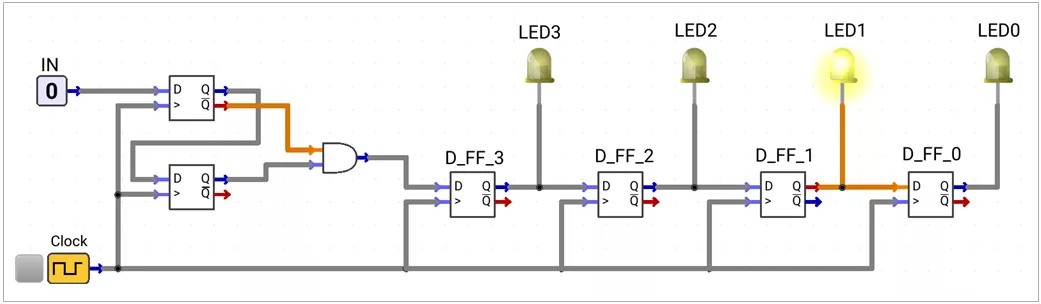
The LED belt uses a 4-bit right shift register to create a moving-light effect.

Each register output is connected to one active-HIGH LED:

  • Q3 → LED3
  • Q2 → LED2
  • Q1 → LED1
  • Q0 → LED0

An active-HIGH output falling-edge detector monitors input IN.

Fig. 10: LED Belt Circuit

led-belt-using-right-shift-register

Circuit Behaviour

  • Normally, the edge-detector output remains 0.
  • When IN changes from 1 → 0, the detector generates one HIGH pulse.
  • This HIGH bit enters the serial input of the shift register.
  • At every clock edge, the HIGH bit moves one position toward the LSB.
  • The connected LEDs show the position of the stored HIGH bit.

Table 8: LED Belt Example

Clock EventRegister Output Q3Q2Q1Q0Glowing LED
Falling edge detected1000LED3
Next clock0100LED2
Next clock0010LED1
Next clock0001LED0

Only one HIGH pulse is inserted for one falling edge. Therefore, one LED moves through the belt after each clock.


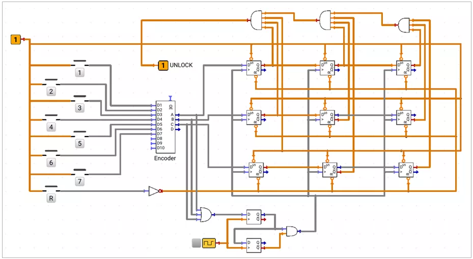
Digital Lock

The digital lock stores a sequence of three button presses and compares it with the correct code:

5 → 1 → 7

Input Section

The circuit contains seven push buttons labelled 1 to 7.

  • A pressed button generates HIGH.
  • Buttons are connected to encoder inputs D1 to D7.
  • The encoder produces outputs A, B, C, and D.
  • Output D is unused.
  • Outputs A, B, and C form the 3-bit button code.

Button-Press Detection

The signal: A + B + C

becomes HIGH when an encoded button value is present.

This signal is connected to an active-HIGH output rising-edge detector.

When a button is pressed:

  • A + B + C changes from 0 → 1.
  • The edge detector generates one HIGH pulse.
  • This pulse is connected to the clock inputs of all PIPO registers.
  • Only one register update occurs for each button press.

Sequence Storage

The circuit uses three 3-bit PIPO registers to store three encoded button values.

The registers store the entered button sequence. The stored values are checked after each entry.

Code Matching

A combinational circuit is connected after each PIPO register.

Each circuit produces HIGH only when its stored 3-bit value matches the required button value:

  • First required value: 5
  • Second required value: 1
  • Third required value: 7

The three match signals are combined to generate UNLOCK.

Table 9: Digital Lock Code Check

Stored EntryRequired ButtonMatch Output
First entry5HIGH when value is 5
Second entry1HIGH when value is 1
Third entry7HIGH when value is 7

When all three stored values match:

UNLOCK = 1

Reset Operation

The R push button shifts the code in next register. It works similar to "0".

Complete Working

  1. The user presses one button from 1 to 7.
  2. The encoder converts the button number into a 3-bit code.
  3. The rising-edge detector generates one clock pulse.
  4. The PIPO registers record the button entry.
  5. The process repeats for three button presses.
  6. The combinational circuits check the stored sequence.
  7. UNLOCK becomes HIGH only when the entered code is 517.

Fig. 11: Digital Lock Circuit using Registers

digital-lock-using-registers