Transistor Quick Reference Guide
What is a BJT?
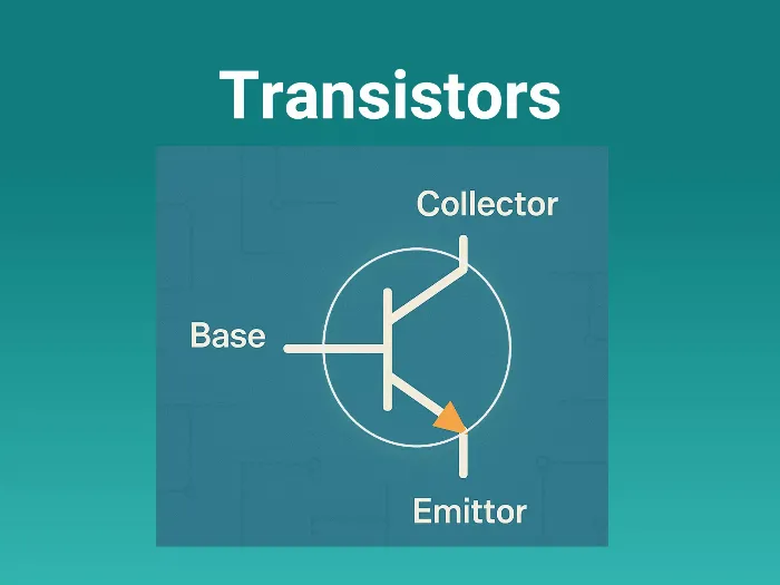
A BJT (Bipolar Junction Transistor) is a three-terminal semiconductor device used to amplify or switch electronic signals. It is one of the most fundamental active components in electronics.
Key Points:
- Three terminals: Base (B), Collector (C), Emitter (E).
- Two types: NPN and PNP — defined by the semiconductor layer arrangement.
- Current-controlled device: A small current into the base controls a much larger current between collector and emitter.
- Gain (hFE or β): The ratio of collector current to base current.
- VBE (Base-Emitter Voltage): The forward voltage needed to turn on the transistor — approximately 0.6–0.7V for silicon BJTs.
IC = hFE × IB
Where:
IC = Collector current,
IB = Base current,
hFE = DC current gain (typically 20–500 depending on the transistor).
Practical Use Cases of BJTs
- Switching – Turning loads ON/OFF using a small control signal (e.g., relay driver, LED driver from MCU GPIO).
- Signal Amplification – Amplifying small analog signals in audio, sensor, and communication circuits.
- Current Sourcing/Sinking – Driving loads that require more current than a microcontroller pin can supply.
- Darlington Pair – Two BJTs cascaded for very high current gain, used in motor drivers and solenoid control.
- Current Mirror – Providing matched, stable current sources in analog IC design and precision circuits.
- Voltage Regulation – Pass transistor in linear voltage regulators.
- Oscillators – Generating waveforms in Colpitts, Hartley, and astable multivibrator circuits.
- Level Shifting – Interfacing between different voltage domains (e.g., 3.3V MCU to 12V load).
Types of BJTs
A. Based on Polarity
| Type | Image | Symbol | Description | Current Flow |
| NPN |  | 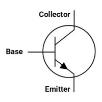 | Most commonly used. Current flows from collector to emitter when base is driven high. Easier to use in common-emitter switching. | Conventional current: C → E. Base current into the base. |
| PNP | 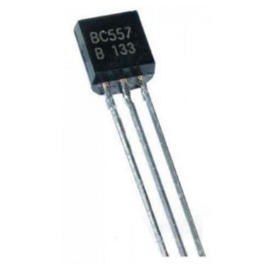 | 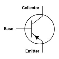 | Current flows from emitter to collector when base is pulled low relative to emitter. Used for high-side switching. | Conventional current: E → C. Base current out of the base. |
When to use NPN vs. PNP:
- NPN — Low-side switching (load between VCC and collector). More common, wider selection.
- PNP — High-side switching (load between collector and ground). Useful when the load must be connected to ground.
B. Based on Application / Construction
| Type | Image | Description | Common Examples |
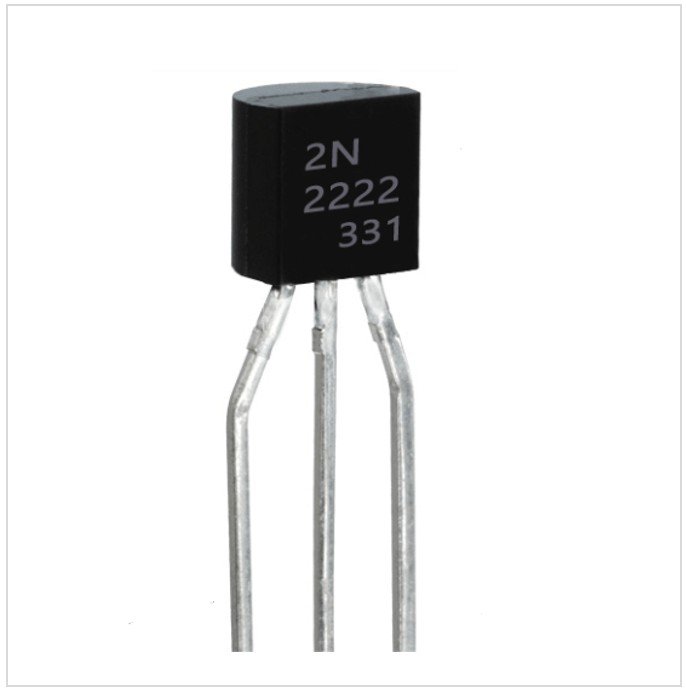
| Small-Signal BJT | 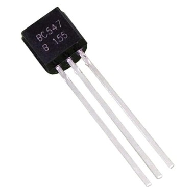 | General-purpose, low-power transistors for switching and amplification. IC typically < 500mA. | 2N2222 (NPN), 2N2907 (PNP), BC547 (NPN), BC557 (PNP) |
| Power BJT | 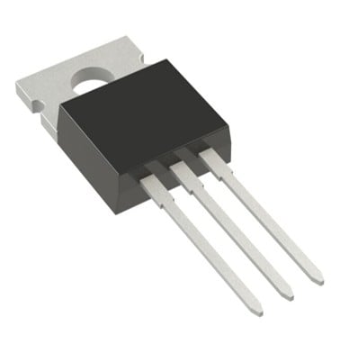 | High-current, high-voltage transistors for power switching, motor control, and regulation. IC from 1A to tens of amps. | TIP31 (NPN), TIP32 (PNP), TIP41 (NPN), TIP42 (PNP), 2N3055 (NPN) |
| Darlington Transistor | 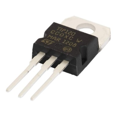 | Two BJTs in a single package for very high gain (hFE = 1000–20,000). Higher VCE(sat) than single BJTs. | TIP120 (NPN), TIP125 (PNP), BC517 (NPN) |
| Digital Transistor (Pre-biased) |  | Built-in base resistors — can be driven directly from MCU GPIOs without external biasing components. | DTC114 (NPN), DTA114 (PNP), PDTC124 series |
| Phototransistor | 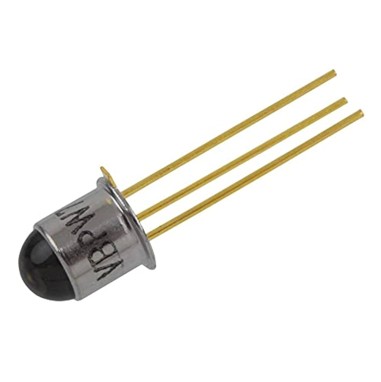 | Light-sensitive BJT where base current is generated by photons. No base lead needed in most applications. | PT334-6C, SFH 309 |
| RF / High-Frequency BJT |  | Optimized for high-frequency amplification with high fT (transition frequency). Used in RF amplifiers, oscillators. | BFR92A, 2N5109, MMBT3904 |
| Matched Pair / Array | 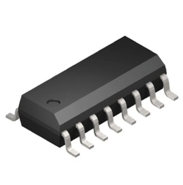 | Two or more BJTs thermally matched in a single package for precision analog circuits (current mirrors, diff amps). | MAT12, DMMT3904 |
Key Specifications
Primary Selection Parameters
1. DC Current Gain (hFE or β) Ratio of collector current to base current. Determines how much base current is needed to drive the desired load current. Typical range: 20–500 for standard BJTs, 1000–20,000 for Darlingtons.
Important: hFE varies significantly with collector current, temperature, and from unit to unit. Always design for the minimum guaranteed hFE in the datasheet, not the typical value.
2. Maximum Collector Current (IC(max)) The absolute maximum continuous current through the collector. For small-signal BJTs, typically 100–800mA. For power BJTs, 1A to 15A+. Always operate well below this limit.
3. Collector-Emitter Saturation Voltage (VCE(sat)) The voltage drop across the transistor when fully ON (saturated). Lower is better for switching efficiency. Typical values: 0.1–0.3V for small-signal, 0.5–1.5V for power BJTs, 1–2V for Darlingtons.
4. Maximum Collector-Emitter Voltage (VCEO) Maximum voltage the transistor can block between collector and emitter when OFF. Must exceed the circuit's supply voltage with margin. Common values: 30V, 45V, 60V, 100V, 300V+.
5. Power Dissipation (PD) Maximum total power the transistor can dissipate as heat. Depends on the package and heatsinking. TO-92: ~0.5W. TO-220: 1–2W (free air), up to 30–65W with heatsink.
6. Transition Frequency (fT) The frequency at which current gain drops to 1. Indicates the transistor's useful frequency range. For audio: fT > 50 MHz is fine. For RF: fT in the GHz range needed. Not critical for DC switching applications.
Secondary Parameters
7. VBE (Base-Emitter Voltage) — Forward voltage to turn on, ~0.6–0.7V for silicon. Needed for biasing calculations.
8. VCBO (Max Collector-Base Voltage) — Maximum reverse voltage across collector-base junction. Usually higher than VCEO.
9. Thermal Resistance (RθJA / RθJC) — How well the device dissipates heat. Lower is better. Critical for power BJTs — determines if a heatsink is needed.
10. Safe Operating Area (SOA) — Graph showing the safe combinations of VCE and IC. Important for linear operation (regulators, audio output stages) where the transistor is not fully saturated.
Example: 2N2222A Specifications
| Specification | Value |
| Type | NPN |
| VCE Breakdown (Max) | 40V |
| IC (max) | 600mA |
| hFE | 100 @ 150mA, 10V |
| VCE(sat) | 1V @ 50mA, 500mA |
| PD | 625 mW |
| fT | 250 MHz |
| Package | TO-92, TO-18, SOT-23 (MMBT2222A) |
BJT Packages
Through-Hole
| Package | Image | Description |
| TO-92 |  | Most common small-signal package. ~0.5W. Used for BC547, 2N2222, 2N3904, etc. |
| TO-220 | 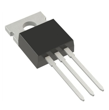 | Power package with heatsink tab. 1–2W free air, up to 30–65W with heatsink. TIP31, TIP41, BD139. |
| TO-3 | 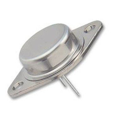 | Heavy-duty metal can for high-power applications. 2N3055. Being replaced by TO-247 in newer designs. |
| TO-247 | 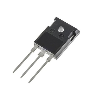 | High-power plastic package. MJL21194. Common in audio power amplifiers and power supplies. |
| TO-126 | 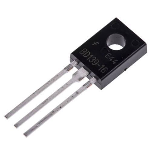 | Mid-power package. BD135/BD136. Smaller than TO-220 but higher power than TO-92. |
Surface-Mount (SMD)
| Package | Image | Description |
| SOT-23 | 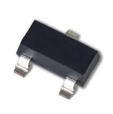 | Most common SMD small-signal package. MMBT3904, MMBT2222A. ~0.35W. |
| SOT-89 | 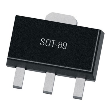 | Medium-power SMD. Better thermal dissipation than SOT-23. ~1W. |
| SOT-223 |  | Higher power SMD with exposed pad. Up to ~1.5W. |
| DPAK (TO-252) | .jpg) | SMD power package. Up to ~2W+ with PCB copper. |
| SC-59 / SC-70 | 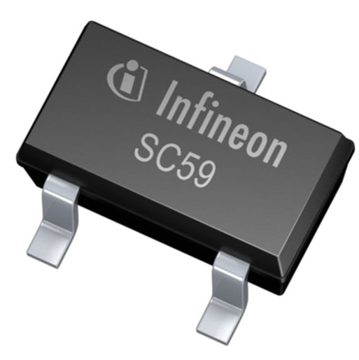 | Ultra-small packages for digital/pre-biased transistors. |
Naming Convention
BJTs follow several standard naming systems:
Naming Convention
- 2N (JEDEC, American): General-purpose BJTs. e.g., 2N2222, 2N3904, 2N3055.
- BC/BD/BF (Pro-Electron, European): B = Silicon; C = low-power, D = power, F = high-frequency. e.g., BC547, BD139, BFR92.
- 2SA/2SB/2SC/2SD (Japanese): A/B = PNP, C/D = NPN (A/C high-freq, B/D low-freq). e.g., 2SC1815, 2SA1015.
- TIP (TI Power): Power BJTs and Darlingtons. e.g., TIP31, TIP120.
- MMBT (SMD): SMD version of a 2N part. e.g., MMBT3904 = 2N3904 in SOT-23.
How to Select a BJT
1. Determine NPN or PNP NPN for low-side switching (most common). PNP for high-side switching.
2. Voltage Rating (VCEO) Must exceed your supply voltage with margin. Use at least 1.5–2× the circuit's maximum VCE.
3. Current Rating (IC) Must handle the load current. Select for at least 1.5× the actual load current.
4. Calculate Base Current Needed IB = IC / hFE(min). Use the minimum hFE from the datasheet. For switching, overdrive the base (force β of 10–20 for guaranteed saturation) so the transistor fully saturates.
5. Check VCE(sat) Ensure the saturation voltage is acceptable for your application. A high VCE(sat) means more power lost as heat in the transistor. Darlingtons have notably higher VCE(sat) (1–2V).
6. Power Dissipation P = VCE × IC. In saturation: P ≈ VCE(sat) × IC. Make sure this is within the device's PD rating at your ambient temperature. Add a heatsink if needed for power BJTs.
7. Speed / Frequency For DC switching, fT doesn't matter much. For audio or RF, ensure fT is well above your operating frequency (at least 10×).
8. Package TO-92 for prototyping and low-power. SOT-23 for production SMD. TO-220/TO-247 for power. Match package to your power dissipation and PCB needs.
Common Design Mistakes
Using typical hFE instead of minimum — hFE varies widely. Designing with the typical value means some units won't saturate fully, leading to overheating or incomplete switching.
Forgetting the base resistor — Without a base resistor, excessive base current can destroy the transistor or the driving MCU pin. Always calculate and include a base resistor.
No flyback diode when driving inductive loads — Relays, solenoids, and motors produce back-EMF spikes that destroy the transistor. Always use a flyback diode across the inductive load.
Using a Darlington where VCE(sat) matters — Darlingtons have 1–2V VCE(sat). In low-voltage circuits (e.g., 3.3V or 5V), this causes significant power loss. Use a single BJT or MOSFET instead.
Ignoring thermal limits — A transistor that's within its IC rating can still overheat if power dissipation exceeds the package rating. Always check P = VCE × IC against PD.
Using a BJT where a MOSFET is better — For high-current switching loads, MOSFETs are generally more efficient (lower on-resistance, voltage-driven). BJTs are better for analog amplification, low-cost switching, and current-controlled applications.
Real-World Design Examples
1. Relay / Solenoid Driver (NPN Switch) MCU GPIO → base resistor → NPN transistor (e.g., 2N2222 or BC547). Collector to relay coil, emitter to GND. Flyback diode across the relay coil. The MCU pin sources only ~0.5–1mA into the base, while the transistor switches 50–200mA through the relay.
2. LED Driver Array Multiple LEDs in series/parallel driven by a single BJT. Useful when the MCU can't supply enough current directly. A BC337 (up to 800mA) can drive several LED strings.
3. Motor Driver (Darlington Pair) TIP120 NPN Darlington driving a small DC motor. Requires only ~1mA base current to switch 1–2A through the motor. Include a flyback diode. Note the ~1.5V VCE(sat) drop.
4. Audio Preamp Stage BC547 or 2N3904 in common-emitter configuration with biasing resistors. Amplifies microphone or sensor signals before feeding to an ADC or audio amplifier IC.
5. Current Source BJT with emitter resistor provides a stable current to an LED or sensor, less dependent on supply voltage variations than a simple resistor.
6. Level Shifter (3.3V to 12V) NPN transistor with collector pull-up to 12V. 3.3V MCU signal turns the transistor on/off, producing a 12V-compatible output for driving peripherals.
BJT vs. MOSFET — When to Use Which
| Feature | BJT | MOSFET |
| Drive Type | Current-driven (base current) | Voltage-driven (gate voltage) |
| Input Impedance | Low (draws base current) | Very high (virtually no gate current in DC) |
| Switching Speed | Moderate (storage time limits speed) | Fast (no minority carrier storage) |
| On-State Loss | VCE(sat) × IC (relatively fixed drop) | RDS(on) × I² (resistive, varies with current) |
| Low-Current Efficiency | Better (low VCE(sat) at small currents) | Can be worse (RDS(on) × I² still present) |
| High-Current Efficiency | Worse (VCE(sat) rises, base drive increases) | Better (lower total loss with low RDS(on)) |
| Cost | Generally cheaper for small-signal | Comparable; power MOSFETs can be cheaper in high-current |
| Analog/Linear Use | Excellent (smooth, predictable gm) | Usable but BJTs are preferred for precision analog |
| Thermal Behavior | Negative temp coefficient (risk of thermal runaway) | Positive temp coefficient (self-stabilizing) |
| Gate/Base Protection | Robust (can tolerate moderate abuse) | Sensitive (gate oxide can be damaged by ESD/overvoltage) |
| Best For | Analog amplification, low-cost switching, current sources, sensor interfaces | High-current switching, power conversion, high-frequency switching, battery-powered designs |
Symbols
Concept understood? Let's apply and learn for real